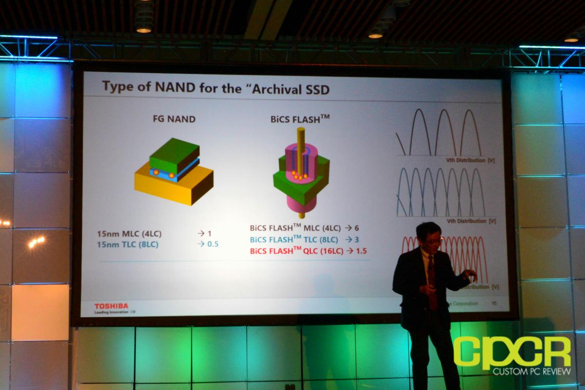
QLC (Quadruple Level Cell), which is also 4-bit MLC, has been announced by Toshiba, vertically stacked of course. It features 4-bit-per-cell, quadruple-level cell (QLC), technology and enables larger (768Gb) die capacity than the company’s third-generation 512Gb 3-bit-per-cell, triple-level cell (TLC).
It also makes a 1.5TB device with a 16-die stacked architecture in a single package possible (the industry’s largest capacity).
Toshiba's new QLC BiCS FLASH device features a 64-layer stacked cell structure and achieves the world's largest die capacity3 (768Gb/96GB). QLC flash memory also enables a 1.5-terabyte (TB) device with a 16-die stacked architecture in a single package – featuring the industry's largest capacity4. This is a fifty percent increase in capacity per package when compared to Toshiba's earlier announcement of a 1TB device with a 16-die stacked architecture in a single package – which also offered the largest capacity in the industry at the time.
The technical challenges posed by QLC technology needed to be overcome, as increasing the number of bits-per-cell by one within the same electron count requires twice the accuracy of TLC technology. Toshiba has combined its advanced circuit design and leading 3D flash memory process technology to overcome this challenge, successfully creating the world's first QLC 3D flash memory.
Additionally, Toshiba has announced the development of its 96-layer BiCS FLASH 3D flash, the 4thgeneration of its industry leading 3D memory. Samples of the new 96-layer product, which is a 256 gigabit (32 gigabyte) TLC device, are scheduled for the second half of 2017, with mass production targeted for 2018.
Samples of the new 96-layer product, which is a 256 gigabit (32 gigabytes) device, are scheduled for release in the second half of 2017 and mass production is targeted for 2018. The new device meets market demands and performance specifications for applications that include enterprise and consumer SSD, smartphones, tablets and memory cards.
Going forward, Toshiba Memory Corporation will apply its new 96-layer process technology to larger capacity products, such as 512 gigabit (64 gigabytes) and 4-bit-per-cell (quadruple-level cell, QLC) technology, in the near future.
The innovative 96-layer stacking process combines with advanced circuit and manufacturing process technology to achieve a capacity increase of approximately 40% per unit chip size over the 64-layer stacking process. It reduces the cost per bit, and increases the manufacturability of memory capacity per silicon wafer.
Since announcing the world’s first[2] prototype 3D flash memory technology in 2007, Toshiba Memory Corporation has continued to advance development of 3D flash memory and is actively promoting BiCS FLASH™ to meet demand for larger capacities with smaller die sizes.
This 96-layer BiCS FLASH™ will be manufactured at Yokkaichi Operations in Fab 5, the new Fab 2, and Fab 6, which will open in summer 2018.


