Samsung surpasses TSMC to become the first manufacturer to begin 3nm chip manufacturing. The news concerning the node production technique was made last month, but Samsung confirmed the first shipment of 3nm chips this week.
The new lithography promises higher performance and 45% less power consumption. According to an official press release, the South Korean manufacturer celebrated the achievement at a special event for about 100 people, including South Korea's Minister of Trade, Industry and Energy, Changyang Lee.
Samsung Electronics' foundry division expressed its ambition to strengthen the competitiveness of its business through mass production of the 3nm process and preventive casting technology, along with the confidence that they would 'advance innovative technology to become the World's greatest.
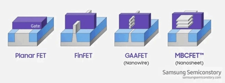
The existence of the GAA (Gate-All-Around) transistor design is the most notable feature of the new chipsets. GAA is a FinFET advancement that enables the foundry to choose transistors without impacting the chip's capacity to transmit electricity. As a result, the efficiency of semiconductors should increase significantly. According to Samsung, the initial wave of 3nm chips would have a 45 percent decrease in power consumption and a 23 percent boost in performance in a 16 percent smaller space than 5nm processors.
Despite these advancements, Samsung claims it is already working on the second generation of 3nm circuits that would lower power consumption by 50% while providing 30% more performance in a 35% smaller space. So far, the business has not revealed who acquired the first shipment of its 3nm chips, although moving ahead of TSMC is undoubtedly a significant move for Samsung.


