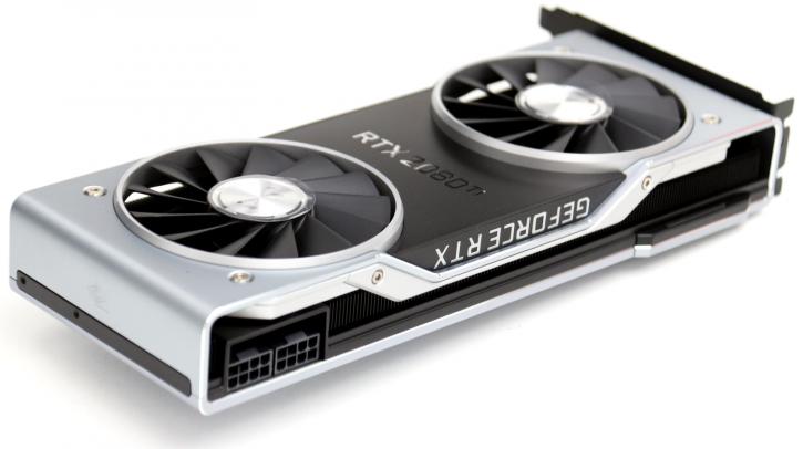
As GDC closes in, most people do expect some NVIDIA Ampere announcements during the keynote, time will tell. Meanwhile, some (and we assume it is Ampere) specs and benchmarks already have leaked from HPC parts. New info was spotted on the web though.
With the some benchmark entries spotted I already explained that most GPU work in a multitude's of that eight (bits/bytes), and that I would not be surprised to see 128 Shader clusters (CUs) and thus a possible 8192 shader cores for a fully enabled GPU. While it is nothing more than a user posting some info on a forum, new speculation is drawing some attention. A Chinese forum called Stage1 apparently has shared some reliable info in the past, and this round he talks about a chip called 'ga100', And GA obviously would be GeForce Ampere. Here's what he posted and galls GA100:
- 128SM, 8192cuda, 24 / 48GB HBM2e, boost frequency up to 2.2Ghz, double the tensor core, 300W TDP
GA100 would get far more compute performance then expected, the 7nm fabbed GA100 would indeed get 8192 cores and thus 128 CUs, meaning NVIDIA if pretty much going monolithic and doubles up on their transistor budget, which going from 12nma and 14nm to 7nm is very possible. Very interesting is the mention of a boost clock up-to 2200 MHz, which seems high especially with a 300W TDP.
All that in combination with 24, 32 or even 48 GB of HBM2e graphics memory would/could deliver 32 teraflops of performance. Obviously we're talking data center and supercomputer centric products here, but Ampere paves the way architecture wise for the consumer products as well. Apparently the number of tensor cores would double up as well.
Relativity can be a bitch - of course, remember, this info is based upon one post in a forum. Grab some salt, but with the number of leaks and GDC so close, I can't rule out this info to be false.
Nvidia Ampere GA100-GPU would get 8192 cores and boost speed up to 2200 MHz


