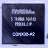
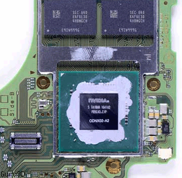
Analysis from Chipworks shows that the Nintendo Switch makes use of a Nvidia Tegra X1 SoC, much like the one used in the Shield that we reviewed yesterday. The usage of this SoC is not a surprise but never was openly admitted by Nvidia and Nintendo. Many assumed the unit would use a custom designed SoC.
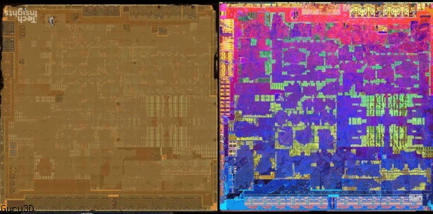
Here's techinsights with their update:
After subsequent processing of the GPU from the Nintendo Switch, we have determined that the processor is the Nvidia Tegra T210. The T210 CPU features 4 Cortex A57 and 4 Cortex A53 processor cores and the GPU is a GM20B Maxell core. Download the high resolution image here.
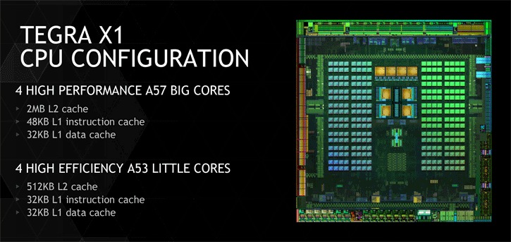
The unit is based upon an 8-core Tegra X1 SoC (64-bit) which is an in-house Nvidia ARM SoC from the Tegra series. It features what is called a BIG little setup that has been arranged as four ARM Cortex-A57 processor cores and then four ARM Cortex-A53 cores.
The big A57 cores have more L2 cache (2MB) plus slightly bigger instruction and data-caches. The unit houses 256 shader/stream/cuda processors based on an all too familiar Maxwell architecture, the codename for the SoC is GM20B. If you look at the upper screenshot, you can literally count the 256 cores arranged in 32 sets of 8. So albeit it won't be high-end gaming, simple Android games will be plenty fast thanks to this design. Despite what many people think, it's not a 28nm fab but actually is one of the few products fabbed on 20nm.
- CPU: ARMv8 ARM Cortex-A57 (1.9 Ghz) quad-core + ARM Cortex-A53 quad-core (64-bit).
- GPU: Maxwell-based 256 core GPU
- MPEG-4 HEVC & VP9 encoding/decoding support
- TSMC 20 nm process
- Power consumption less than 10 Watts
Nintendo Switch Houses a Nvidia Tegra X1-SoC


