What's SATA | NVMe | NAND Types
NVMe
NVMe is also known as Non-Volatile Memory Express or the Non-Volatile Memory Host Controller Interface Specification. The idea behind NVMe is to improve the storage stack by optimizing the way an application accesses a Flash device. NVMe cuts corners by removing components within the I/O path like that suitable old-fashioned RAID controller. NVMe leverages PCIe as transport media, which offers high bandwidth and a direct route to the host's CPU and memory. This, in turn, removes another potential bottleneck, the limited bandwidth of SAS, or the latest SATA3 connection. NVMe makes use of your PCI-Express lanes, and as you know... the newest gen 3 PCIe lanes are fast and thus lift the bottleneck that SATA3 has. Moving from PCIe Gen 2 to Gen 3 doubles the bandwidth available to the add-on cards installed, from 500 MB/s per lane to 1 GB/s per lane. PCIe 4.0 once again doubles that up, Obviously, the hardware you use needs to be Gen 4.0 compatible.
| PCIe Version | Line Code | Transfer Rate | x1 Bandwidth | x4 | x8 | x16 |
|---|---|---|---|---|---|---|
| 1.0 | 8b/10b | 2.5 GT/s | 250 MB/s | 1 GB/s | 2 GB/s | 4 GB/s |
| 2.0 | 8b/10b | 5 GT/s | 500 MB/s | 2 GB/s | 4 GB/s | 8 GB/s |
| 3.0 | 128b/130b | 8 GT/s | 984.6 MB/s | 3.938 GB/s | 7.877 GB/s | 15.754 GB/s |
| 4.0 | 128b/130b | 16 GT/s | 1.969 GB/s | 7.877 GB/s | 15.754 GB/s | 31.508 GB/s |
So that the NVMe M.2 units use whatever they are assigned; most motherboards and units now can connect on an x4 link, so that Gen 4.0 x4 link of yours can handle a total bandwidth of 16 GB/s (bi-directional) in PCIe Gen 4.0 mode. In contrast, the old Gen 1.0 x16 slot would be capable of 2GB/sec (bi-directional). That bandwidth combined with fast NAND and a top-notch controller can allow for massive storage speeds.
SATA 3 (6Gbps)
SATA 6G (SATA 3), the latest revision of your SATA storage unit connectors, will increase the bandwidth on the SATA controller from 3 Gbit/sec to 6 Gbit/s. For a regular HDD that is not very important. But with the tremendous rise of fast SSD drives, this is a significant plus. Typically we get 3000 Mbit/s : 8 = 375 MB/s bandwidth minus overhead, tolerances, error-correction and random occurrences. SATA 3 doubles it up, as such we get 6000 Mbit/s : 8 = 750 MB/s (again deduct overhead, tolerances, error-correction and random occurrences) of available bandwidth for your storage devices. As you can understand, with SSDs getting faster and faster that's just a much warmed and welcomed increase of bandwidth. Put Sata3 in RAID and you'll have even more wicked performance at hand. Most motherboards offer only two ports per controller though, so you are (for now) limited to RAID 0 and RAID 1 (stripe or mirror).
What is NAND?
Flash memory is an electronic non-volatile computer storage medium that can be electrically erased and reprogrammed. Introduced by Toshiba in 1984, flash memory was developed from EEPROM (electrically erasable programmable read-only memory). There are two main types of flash memory, which are named after the NAND and NOR logic gates. The NAND type is primarily used in main memory, memory cards, USB flash drives, solid-state drives (those produced in 2009 or later), and similar products, for general storage and transfer of data.
NAND Types
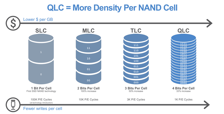
In the beginning, memory cells stored just a single bit of information. However, the charge on the floating gate can be controlled with some level of precision, allowing the storage of more information than just 0 and 1. So you can store more with the same cell? That's easy cost reduction. Based on such an assumption the (Multi-Level Cell) memory came into play. To distinguish them, the old memory type was called SLC - Single Level Cell. In the year 2019 we now differentiate four primary NAND storage wite methods:
- SLC (1 bit per cell written) - the fastest, highest cost
- MLC (2 bits per cell written)
- TLC (3 bits per cell written)
- QLC (4 bits per cell written) - slowest, least cost
The decision of choosing between SLC, TLC, QLC and MLC is driven by many factors such as memory performance, the number of target erase/program cycles and level of data reliability. The MLC memory endurance is significantly lower (around 10,000 erase/program cycles) compared to SLC endurance (around 100,000 erase/program cycles).At the other end of that spectrum is TLC and QLC with roughly 1000 P/E cycles.
Toggle-mode MLC - Toggle-mode MLC is asynchronous NAND that is supposed to provide similar performance as synchronous NAND, but at a lower price. Independent testing has not verified these claims yet. Toggle-mode MLC is also known as double-data-rate asynchronous NAND. Synchronous and asynchronous NAND, based on spec sheets, look remarkably similar in performance. However, they aren't. Synchronous NAND is more expensive than asynchronous. Sync NAND is used when performance is everything, such as with gaming systems.
TLC flash memory (triple-level cell flash) is a type of solid-state NAND flash memory that stores three bits of data per cell of flash media. TLC flash is less expensive than single-level cell (SLC) and multi-level cell (MLC) solid-state flash memory, which makes it appealing for consumer devices that use solid-state storage. The drawbacks to using TLC flash are performance, reliability, and longevity. TLC flash has lower write endurance than both SLC and MLC flash. Generally, the more bits of data the cell has, the fewer write cycles it will support. SLC memory cells can withstand up to 100,000 write cycles before failing. A 2-bit MLC memory cell can typically withstand up to 10,000 write cycles before failing. A TLC memory cell can sustain about 1,000 write cycles before failing, which is why thus far it has been limited to consumer-grade applications.
Ever since 2019 we now also have QLC NAND writes 4 bits per cell. Adding more bits per cell also affects the life-span of the NAND cell, and thus that brings down the number of times it can be written. Much like TLC (Triple-level cell), many new technologies like error-correction mechanisms and wearing have increased the life-span of the respective SSDs. For example, a 500 GB TLC based SSD can quite easily manage a 300TB written before NAND cells start to die off. TLC has roughly a 1000 PE cycles, and that is the claim for QLC as well, a 1000 PE cycles. On 64-layer 4bits/cell NAND technology, companies are achieving 33 percent higher array density compared to TLC, which enables them to produce the commercially available 1 terabit die in the history of semiconductors already.


