The Turing GPU
The Turing GPU
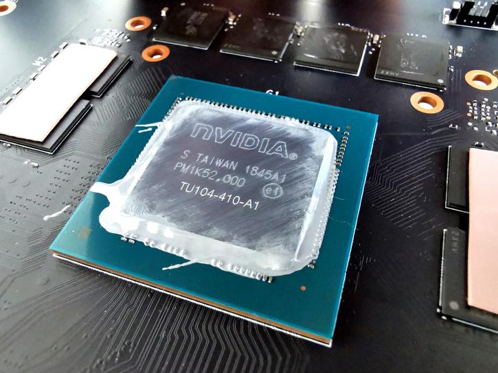
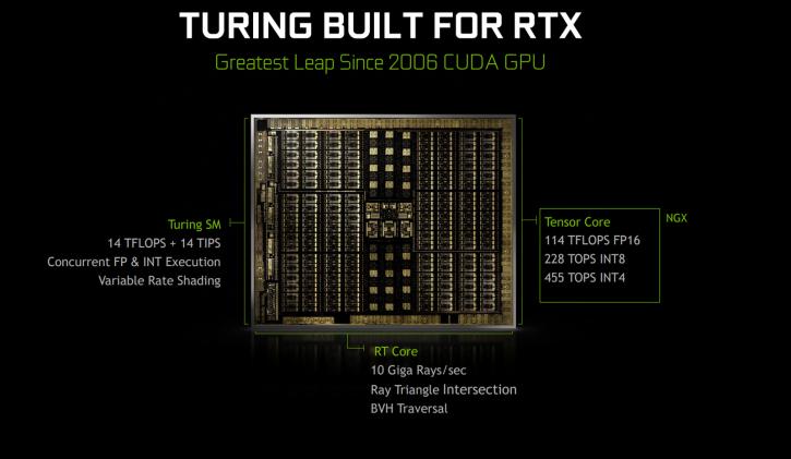
Looking at the Turing GPU, there is a lot of stuff you can recognize, but starting at Turing there certainly have been fundamental block changes in the architecture; the SM (Streaming Multiprocessor) clusters have separated, and now are core separated isolated blocks. Bear in mind that the base building block for all Turing GPUs will be the TU102, that is the flagship GPU that has been used on the GeForce RTX 2080 Ti. The RTX 2080 uses the TU104, the RTX 2060 TU106 and 2070 SUPER also TU104. In essence, the TU106 is the more simplified revision of the TU102, but shares its architecture. It's fabbed at 12nm FFN.
Turing GPU Specifications
Gamers will immediately look at the shader processors, the Quadro RTX 8000 has 4608 of them enabled and, since everything with bits is in multitudes of eight, while looking at the GPU die photos; a TU104 based GeForce RTX 2070 Super has 40 SMs (streaming multiprocessors) each holding 64 cores = 2560 Shader processors. This GPU is fabbed on an optimized 12nm TSMC FinFET+ node and the full GPU is unlocked.
* reference specifications
Turing architecture
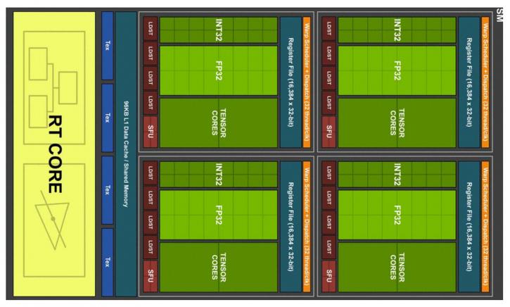
We'll try and be brief here, but Turing is a new and completely overhauled architecture that actually has gotten a new SM (Streaming Multiprocessor) design. As I mentioned, it has a bit of everything, but mostly it hints towards Volta. Two SMs are included per TPC (Texture / Processor Cluster - a group made up of several SMs). Each SM has a total of 64 FP32 Cores and 64 INT32 Cores. Now before you get all confused, yes, that is radically different from Pascal (GeForce series 1000) which had one SM per TPC and 128 FP32 Cores per SM. The Turing SM architecture supports parallel execution of FP32 and INT32 operations, independent thread scheduling similar to the Volta GV100 GPU. That's also described as concurrent execution of FP32 and INT32 operation. Each Turing SM holds eight Turing Tensor Cores. With that out of the way, have a peek at the block diagram below.
Each Turing SM is partitioned into four processing blocks, each holds 16 FP32 Cores, 16 INT32 Cores, two Tensor Cores, one warp scheduler, and one dispatch unit. Each block includes a new L0 instruction cache and a 64 KB register file. The four processing blocks share a combined 96 KB L1 data cache/shared memory. Traditional graphics workloads partition the 96 KB L1/shared memory as 64 KB of dedicated graphics shader RAM and 32 KB for texture cache and register file spill area. Compute workloads can divide the 96 KB into 32 KB shared memory and 64 KB L1 cache, or 64 KB shared memory and 32 KB L1 cache.
Concurrent Execution of Floating Point (fp32) and Integer Instructions (int32)
Turing’s SM initiates a new unified architecture for shared memory, L1, and texture caching. This unified design allows the L1 cache to leverage resources, increasing its bandwidth by 2x per TPC compared to Pascal, and allows it to be reconfigured to grow larger when shared memory allocations are not using all the shared memory capacity. The Turing L1 can be as large as 64 KB in size, combined with a 32 KB per SM shared memory allocation, or it can reduce to 32 KB, allowing 64 KB of allocation to be used for shared memory. Turing’s L2 cache capacity has also been increased. Combining the L1 data cache with the shared memory reduces latency and provides higher bandwidth than the L1 cache implementation used previously in Pascal GPUs. NVIDIA claims these changes in SM enable Turing to achieve 50% improvement in delivered performance per CUDA core. Turing GPUs add larger and faster L2 caches in addition to the new GDDR6 memory subsystem. The TU102 GPU ships with 6 MB of L2 cache, double the 3 MB of L2 cache that was offered in the prior generation GP102 GPU used in the TITAN XP. TU102 also provides significantly higher L2 cache bandwidth than GP102. Like prior generations of NVIDIA GPUs, each ROP partition in Turing contains eight ROP units and each unit can process a single-color sample. A full TU102 chip would contain 12 ROP partitions for a total of 96 ROPs. The RTX 2080 and 2070 have 64 of these.


