The Technology and Specs
Reference technology and specs
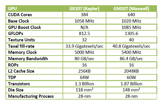
In this segment of the article we will look at the reference (original design) based specs and architecture. The GeForce GTX 750 and 750 Ti are based on Maxwell GPU architecture. The product however uses the GM107 which is based on a 28nm fabrication process. That chip has 1.87 Billion transistors.
Maxwell
NVIDIA’s first-generation “Maxwell” GPU architecture implements a number of architectural enhancements designed to extract even more performance and more power efficiency per watt consumed. The first Maxwell-based GPU is codenamed “GM107” and designed for use in power-limited environments like notebooks and small form factor (SFF) PCs. The first graphics card that is based on the GM107 GPU is the GeForce GTX 750 Ti. Because of GM107’s architectural efficiency, at 1080p resolution a GeForce GTX 750 Ti will have a TDP hovering at merely 60 Watts.
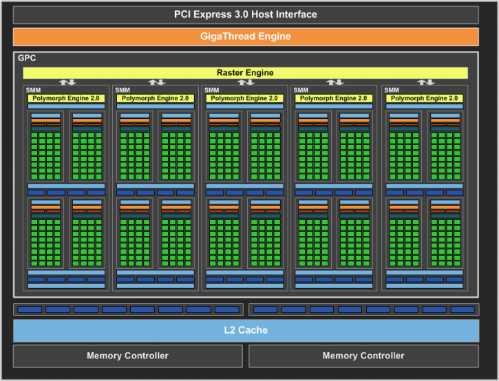
For Maxwell Nvidia applied a new design of Streaming Multiprocessor (SM) with the focus to improve overall performance per watt and performance. The new Maxwell SM architecture now has five SMs in GM107, compared to two in GK107, with only a 25% increase in die area. Maxwell also has a larger L2 cache design; 2048KB in GM107 versus 256KB in GK107. With more cache located on-chip, fewer requests to the graphics card DRAM are needed, thus reducing overall board power and improving performance.
Maxwell implements multiple SM units within a GPC (Graphics Processing Cluster), and each SM includes a Polymorph Engine and Texture Units, while each GPC includes a Raster Engine. ROPs are still aligned with L2 cache slices and Memory Controllers. The GM107 GPU contains one GPC, five Maxwell Streaming Multiprocessors (SM), and two 64-bit memory controllers (128-bit total).
When we peek at NVIDIA's slide decks we see them denoting that the GeForce GTX 750 Ti has been designed for 1080p gaming with medium settings and FXAA. That's true, but please do understand this remains an entry level graphics card series. As far as we are concerned, mainstream will start at the GTX 760.
- The GeForce GTX 650 boasts 384 CUDA (shader) cores (GK107)
- The GeForce GTX 650 Ti boasts 768 CUDA (shader) cores (GK106)
- The GeForce GTX 660 boasts 960 CUDA (shader) cores (GK106)
- The GeForce GTX 660 Ti boasts 1344 CUDA (shader) cores (GK104)
- The GeForce GTX 750 boasts 512 CUDA (shader) cores (GM107)
- The GeForce GTX 750 Ti boasts 640 CUDA (shader) cores (GM107)
GeForce GTX 750
The 1GB GeForce GTX 750 ships with 4 activated SMX units containing 512 Shader Cores and 32 Texture Units. The core clock frequency will be 1020 MHz while it can boost towards 1085 MHz. The memory speed is locked at an 5010 MHz effective data rate based on a 1250 MHz quad data rate for GDDR5 over 128-bit memory bus.
GeForce GTX 750 Ti
The more interesting product will be the GTX 750 Ti which has 5 activated SMX units containing 640 Shader Cores and 40 texture units / 16 rops. The core clock frequency will be 1020 MHz while it can boost towards 1085 MHz. The memory speed is locked at an 5400 MHz effective data rate based on a 1350 MHz quad data rate for GDDR5 over a 128-bit memory bus.
You'll notice that the TDP of these cards is set at a maximum of 60 Watts. Thanks to Maxwell, the GeForce GTX 750 and Ti draw relatively little power. Many GeForce GTX 750 boards are capable of hitting speeds in excess of 1100 MHz easily. The idle power of the GeForce GTX 750 series is merely a few watts, actually 3 to 5W representing terrific in-class idle power. In addition, HD video playback is ~13W, again representing great power consumption. Display outputs include two dual-link DVIs and one mini-HDMI, however this will differ per board partner.
128-bit Memory Interface
The memory subsystem of the GeForce GTX 750 cards are based up-on two 64-bit memory controllers in use (128-bit) with either 1GB or 2GB of GDDR5 memory. The ROP (raster operation) engine was cut down to 16 units. With this release, NVIDIA now has the first Maxwell products on their way. The new graphics adapters are DirectX 11.2 ready.
| GeForce GTX 650 |
GeForce GTX 650 Ti |
GeForce GTX 660 |
GeForce GTX 660 Ti |
GeForce GTX 750 |
GeForce GTX 750 Ti |
GeForce GTX 760 |
|
| Stream (Shader) Processors | 384 | 768 | 960 | 1344 | 512 | 640 | 1152 |
| Core Clock (MHz) | 1058 | 925 | 980 | 915 | 1020 | 1020 | 980 |
| Shader Clock (MHz) | 1058 | 925 | - | - | - | - | - |
| Boost clock (Mhz) | - | - | 1033 | 980 | 1085 | 1085 | 1033 |
| Memory Clock (effective MHz) | 5000 | 5400 | 6008 | 6008 | 5010/5400 | 5400 | 6008 |
| Memory amount | <2048 | <2048 | 2048 | 2048 | 1024 | 2048 | 2048 |
| Memory Interface | 128-bit | 128-bit | 192-bit | 192-bit | 128-bit | 128-bit | 256-bit |
| Memory Type | GDDR5 | GDDR5 | GDDR5 | GDDR5 | GDDR5 | GDDR5 | GDDR5 |
For Maxwell on the 750 series, NVIDIA kept their memory controllers GDDR5 compatible. Memory wise NVIDIA has normal memory volumes due to their architecture. We pass 2 GB as standard these days for most of NVIDIA's series 700 graphics cards in the high range spectrum. We expect most GTX 750 cards to come with 1 GB of graphics memory in order to remain price competitive, the 750 Ti 2 GB models will be roughly 35 USD/EUR more expensive.
Updated Video Capabilities
One of Kepler’s key innovations over prior GeForce GPUs was its hardware-based H.264 video encoder, NVENC. By integrating dedicated hardware circuitry for video encoding/decoding (rather than using the GeForce GPU’s CUDA Cores) NVENC provided a dramatic performance speedup for H.264 encoding while consuming less power. To improve video performance, Maxwell features an improved NVENC block that provides faster encode (6-8X real-time for H.264 vs. 4x real-time for Kepler) and 8-10X faster decode, and thanks to a new local decoder cache, higher memory efficiency per stream for video decoding, resulting in lower power for video decode. Maxwell also features a new GC5 power state that’s been tailored to reduce the GPU’s power consumption specifically for light workload cases like video playback. GC5 is a low power sleep state that provides considerable power savings over prior GPUs for these scenarios.


