Page 2
The C19 CRB reference mainboard![]()
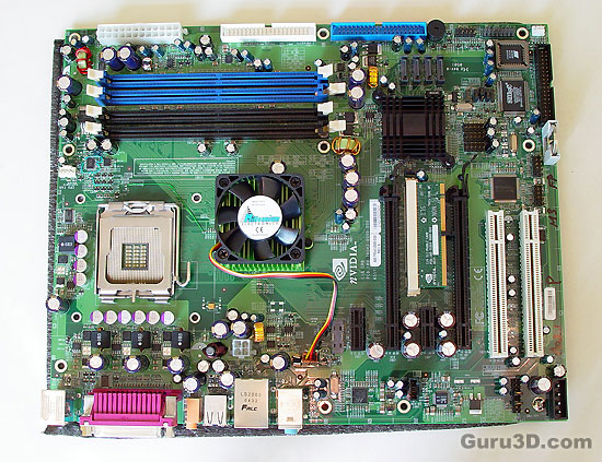
When we take a look at the mainboard photo's we see that it of course is a reference board. Nothing really exciting to look, often too big and often they have quite a number of bugs that still need to be fixed. Hey, these are pre-production engineering samples. And while we certainly had our share of problems (installing a beta nForce driver and not even being able to boot into safe mode is always a good one), I must say that I was really impressed by its stability and performance. Looking at the mainboard you need to know that it can handle a 1066 MHz FSB and likely a little higher. It has native 1 Gigabit Networking, Serial ATA 2, 16x PCI Express (or (2x) 8x lanes PCI-Express in SLI).
Many of you always want to know process size and transistor count for the chips. They are as follows:
-
NVIDIA nForce4 SLI Intel Edition SPP: 0.13 micron; 61 million transistors
-
NVIDIA nForce4 SLI Intel Edition MCP: 0.15 micron; 21 million transistors
For the AMD K8 line NVIDIA was able to do something simple, they effectively moved all functions into a one-chip solution (MCP) while we are familiarized to the traditional mainboard chipset north- and south bridge chips being paired. This was mainly due to the built-in memory controller in the K8 part. Unfortunately when you are going Intel you need to go back to that older solution as the processor does not have a memory controller of its own.. Therefore NVIDIA had to move back to a SPP/MCP combination. Interesting stuff actually as the SPP can handle 20 lanes of PCI Express and has a built-in DDR2 memory controller, which we'll discuss in a tidbit. We believe that there will not be a DDR1 version and/or compatibility, which really is a shame.
The SPP can communicate with the processor through a maximum 1066 MHz front side bus and more entertainingly, it connects to the MCP unit through... HyperTransport, something we know and love on AMD platforms, to my knowledge this is a first for an Intel based platform.
The MCP (call it Southbridge if you will) does not differ from what we see on the AMD nForce4 platform. We see niche gadgets like Active Armor, Serial ATA (2), up-to 10 USB 2.0 ports, AC'97 7.1 Audio and RAID function for both Serial and Parallel ATA. All in all, a mainboard chipset that is versatile and packed with a lot of features.

Codename C19 - The NVIDIA nForce4 SLI Intel Edition reference mainboard. Clearly visible, covered by heatsink and/or fan, are the SPP and passively cooled MCP.

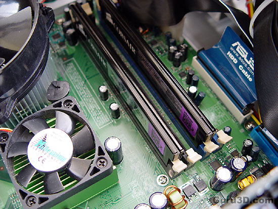
DDR2 is what you need to maximize that memory bandwidth. We however doubt a little that DDR2 will ever be a big success.
