Reference technology and specs
Reference Technology & Specs
So as always, we'll first address the reference technology first. A reference product is a board designed by NVIDIA in this case, it's the baseline template. A product like we tested today, is always based of the reference design and sometimes optimized a little in terms of VRM, PCB design, component usage, clock frequencies, cooling and display outputs. But the building template that the manufacturers work from, is in fact, that reference design.
In this segment of the article we will look at the reference (original design) based specs and architecture. The GeForce GTX 650 Ti Boost is based on the Kepler GPU architecture. The product is using the GK106 which is based on a 28nm fabrication process. You guys all know the GK106 from the GeForce GTX 660 products. That chip has 2.64 Billion transistors.
Now try to follow this:
- There is that regular GeForce GTX 650, and then...
- The GeForce GTX 650 Ti is 40% faster than the GTX 650 on average.
- The GeForce GTX 650 Ti Boost is 40% faster than the GTX 650 Ti on average
768 Shader Processors On The Ti Series
When we peek at NVIDIA's slide decks we see them denoting that the GeForce GTX 650 Ti series has been designed for 1080p gaming with medium settings and FXAA. That's true but please do understand this remains a budget level graphics card.
- The GeForce GTX 650 contains 384 CUDA (shader) cores (GK107)
- The GeForce GTX 650 Ti contains 768 CUDA (shader) cores (GK106)
- The GeForce GTX 650 Ti Boost contains 768 CUDA (shader) cores (GK106)
- The GeForce GTX 660 contains 960 CUDA (shader) cores (GK106)
- The GeForce GTX 660 Ti contains 1344 CUDA (shader) cores (GK104)
- The GeForce GTX 670 contains 1344 CUDA (shader) cores (GK104)
- The GeForce GTX 680 contains 1536 CUDA (shader) cores (GK104)
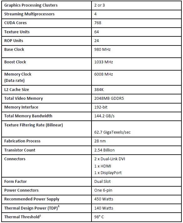
The GeForce GTX 650 Ti Boost ships with 4 activated SMX units containing 768 CUDA Cores and 64 texture units. The graphics core clock speed of the GeForce GTX 650 Ti is 980 Mhz (reference frequency - AIB/AIC partners will ship with higher clocks) with a Boost frequency of 1033 MHz. The GeForce GTX 650 Ti memory speed is locked at an 6000MHz effective data rate based on a 1500 MHz quad data rate for GDDR5.
You'll notice that the TDP of the card is a notch higher, a maximum of 140 watts, however since a segment of the GPU is not used the realistic power consumption will be a tad lower. We measured that to be roughly 135 Watts. The GeForce GTX 650 Ti Boost ships with an external 6-pin power connector. This power connector provides additional headroom for overclocking as well. Many GeForce GTX 650 Ti and Boost edition boards are capable of hitting speeds in excess of 1100 MHz quite easily. The idle power of GeForce GTX 650 Ti Boost is 5W to 10W representing good in class idle power. In addition, HD video playable is ~13W, again representing best in class power consumption.
Display outputs include two dual-link DVI one Display Port and one HDMI connector, however this could be different per board partner.
192-bit Memory Interface
The memory subsystem of the GeForce GTX 650 Ti consisted out of two 64-bit memory controllers in use (128-bit) with either 1GB or 2GB of GDDR5 memory. The Boost edition is getting a nice upgrade, three 64-bit memory controllers are in use offering a 192-bit wide memory bus. And that translates into 144 GB/sec of memory bandwidth. That's pretty sweet actually.
Another change is the ROP (raster operation) engine, this was 16 units and now is 24 similar like it's bigger brother the GeForce GTX 660. The new graphics adapters are of course DirectX 11.1 ready, and that means advantages like DirectCompute, multi-threading, hardware tessellation and the latest shader 5.0 extensions. For your reference here's a quick overview of some of the more recent graphics cards.
| GeForce GTX 650 |
GeForce GTX 650 Ti |
GeForce GTX 650 Ti Boost |
MSI GTX 650 Ti Boost OC |
GeForce GTX 660 |
GeForce GTX 660 Ti |
GeForce GTX 670 |
GeForce GTX 680 |
GeForce GTX 690 |
|
| Stream (Shader) Processors | 384 | 768 | 768 | 768 | 960 | 1344 | 1344 | 1536 | 3072 |
| Core Clock (MHz) | 1058 | 925 | 980 | 1033 | 980 | 915 | 915 | 1006 | 915 |
| Shader Clock (MHz) | 1058 | 925 | - | - | - | - | - | - | - |
| Boost clock (Mhz) | - | - | 1033 | 1098 | 1033 | 980 | 980 | 1058 | 1019 |
| Memory Clock (effective MHz) | 5000 | 5400 | 6008 | 6008 | 6008 | 6008 | 6008 | 6008 | 6008 |
| Memory amount | <2048 | <2048 | 2048 | 2048 | 2048 | 2048 | 2048 | 2048 | 4096 |
| Memory Interface | 128-bit | 128-bit | 192-bit | 192-bit | 192-bit | 192-bit | 256-bit | 256-bit | 256-bit |
| Memory Type | GDDR5 | GDDR5 | GDDR5 | GDDR5 | GDDR5 | GDDR5 | GDDR5 | GDDR5 | GDDR5 |
As you can see the product stack certainly is getting a little crowded. For Kepler, NVIDIA kept their memory controllers GDDR5 compatible. Memory wise NVIDIA offers nice large memory volumes due to their architecture, we pass 2 GB as standard these days for most of NVIDIA's series 600 graphics cards in the high range spectrum. We expect most GTX 650 Ti Boost cards to come with 2 GB of video memory.

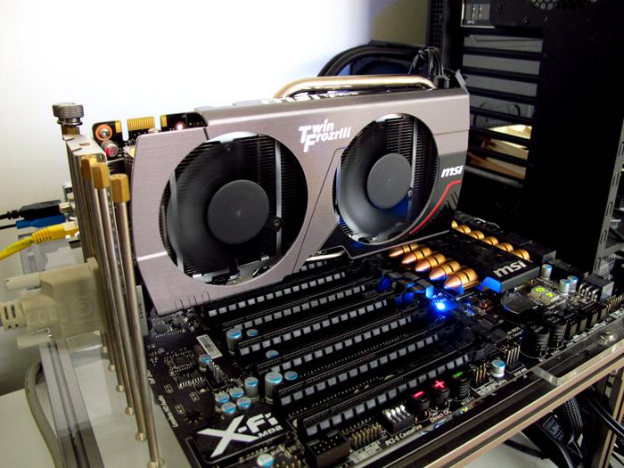
The MSI OC edition SKU is faster due to its core base clock set at 1033/1098 MHz and the memory at 6008 Mhz (effective datarate).


