Product Innards
Product Innards
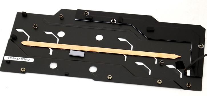
So we take off the back-plate locked in with screws. At the backside there is a copper pipe that touches the rear of the GPU. Basically this functions as a heatspreader, e.g. removing the heat from the backside of the GPU and spreading that heat all over the backplate.
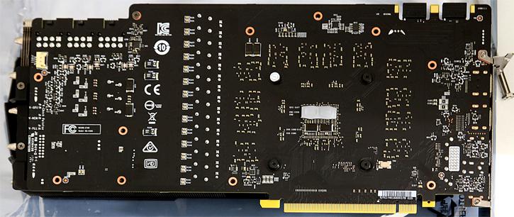
Here we have removed the back-plate. The critical chips that touch the copper pipe have been cushioned with thermal padding.
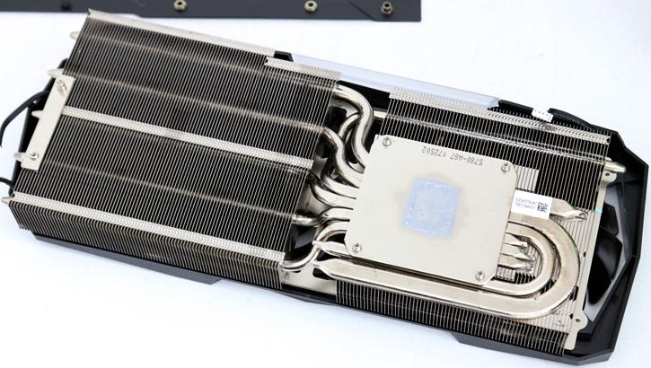
The cooling solution is impressive overall, it uses very thick heat-pipes that pass through a heatsink, with thermal paste tied to the all-copper nickle plated block.
When we flip the PCB it around you can also see that the critical components are covered with a full contact plate. The memory area has padding as well as the phase chokes and thus is cooled.
MSI also did apply padding on top of the GDDR5X, the VRM area as well. Here I have taken off the front and back-plate btw. There is roughly 2 mm space in between PCB and plate on the backside.
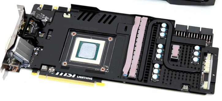
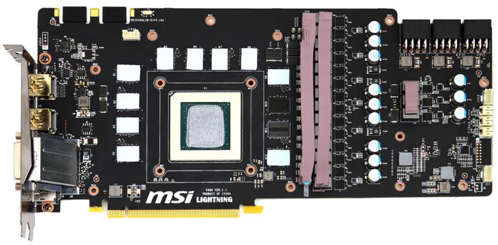
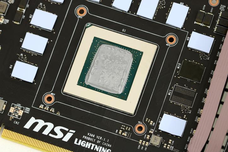
Here we have the front-side of the PCB, clearly visible the GP102 graphics processor from Nvidia covered with thermal interface material. The Nvidia GP102 graphics processor is made based on Pascal architecture at a 16 nm process at TSMC. This bad boy has a transistor count of 12 billion and do not underestimate the die size, that is 471 mm² you are looking at.
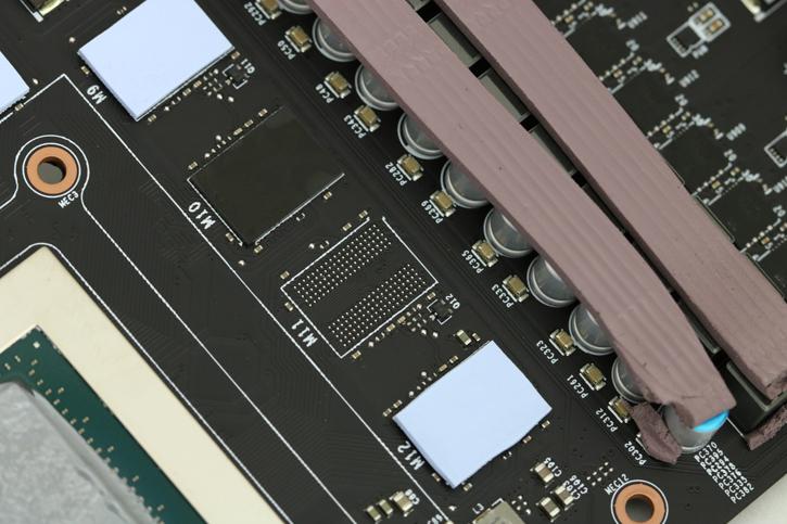
The GDDR5X memory chips are made by Micron and are specced to run at 11,000 MHz GDDR5 (effective data-rate). Tweaked, you are looking at a capability of roughly 12,000 MHz (effective data-rate). These are most likely Micron D9VRL rated at 11 Gbps / 1.35V, however Micron also offers a 12 Gbps IC under the product name D9VRN, I assume it's the first though. It was just too hard to read. BTW That empty SMT trace is for another memory chip (cards that have 12 GB) like the Titan Xp.
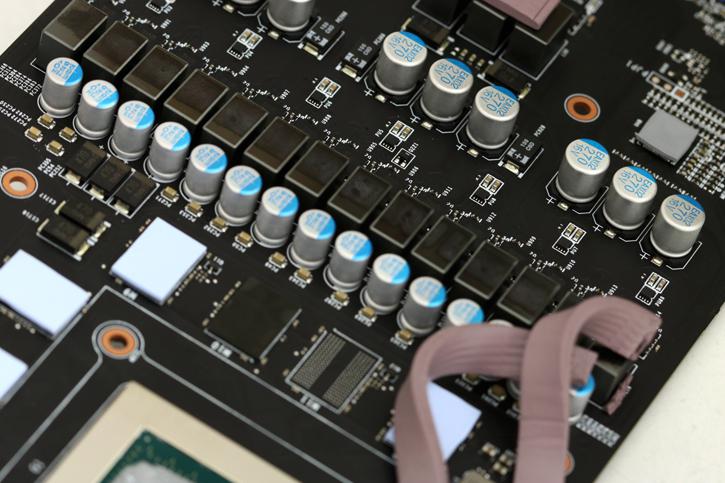
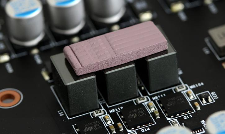
You can count them, 14 phases for the graphics processor, nicely cushioned with thermal padding.
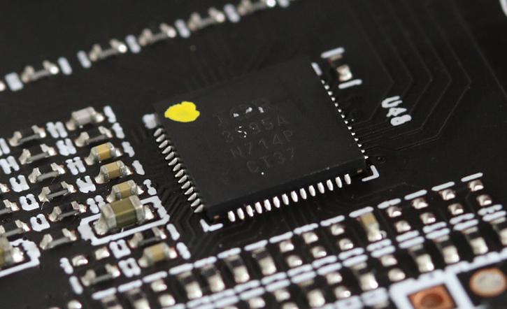
I had to carefully look here, but MSI is using an International Rectifier IR3595A voltage controller, a fairy high-end controller that actually was used on the GeForce GTX 980 Ti Lightning 6GB as well.
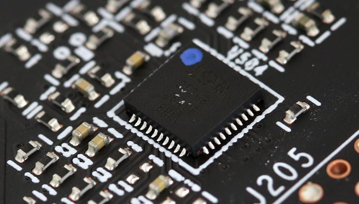
So hard to read, but this is a Infineon / IR International Rectifier dual output digital multi-phase Controller and is designed to be a dual loop digital multi-phase buck controller and functions as dual output 4+1 and 3+2 phase PWM Controllers. It would make sense as this card can support multiple (quad) voltage controls; on the lightning one for GPU, Memory and then two AUX channels (see overclocking chapter).
The board using 14 phases for the GPU but there are three others, for memory (see photo above). And no that is not chewing gum, it is thermal cushioning. As you'll see later in thermal imaging, this board is seriously properly cooled.
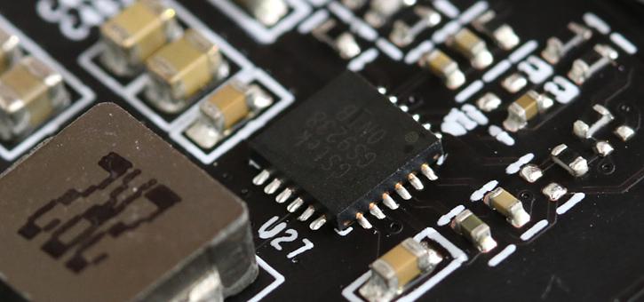
And that would be a GStek GS9238 single buck converter - capable of 8A output each. Buck controller regulators allow for selectable power phases.

