Sandy Bridge processors
A bit of History
Sandy Bridge was the first generation of processors for socket 1155 and shared a lot of innovation including an IGP and ring bus design. To date, the ring bus design is used processors up-to but not including high-end Skylake-X which moved towards its mesh structure. Let's do the steps and inter architecture name changes, as there have been seven steps:
| Westmere | Core i | Tick | 32 nm | 2010 |
| Sandy Bridge | Core i 2xxx | Tock | 32 nm | 2011 |
| Ivy Bridge | Core i 3xxx | Tick | 22 nm | 2012 |
| Haswell | Core i 4xxx | Tock | 22 nm | 2013 |
| Broadwell | Core i 5xxx | Tick | 14 nm | 2014 & 2015 for desktops |
| Skylake | Core i 6xxx | Tock | 14 nm | 2015 |
| Kabylake | Core i 7xxx | Tock | 14 nm | 2016 |
| Coffee lake | Core i 8xxx | TOCK | 14 nm | 2017 |
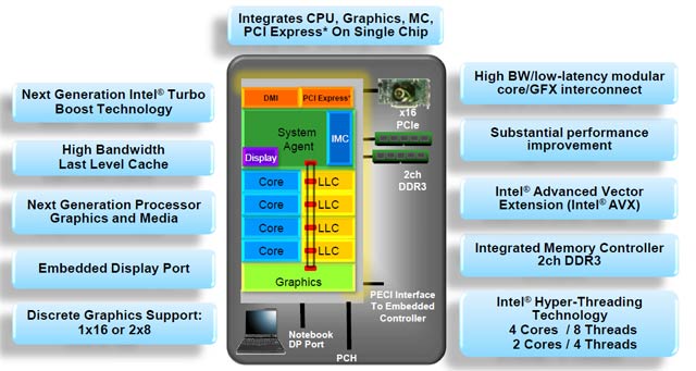
Sandy Bridge was a completely new architecture. The overall processor performance staggered us all and inside the die, merged deeply in there, we spotted this new thing, an integrated GPU with twice the performance of the last generation we saw from Clarkdale processors. It was an improvement in the low-end segment. There was more though, we noticed a new AVX instruction set extension and also spotted an updated Turbo engine allowing much more efficient per core performance and clock frequencies. Finally, power consumption was another factor that was addressed. Paired with Sandy bridge came new motherboard chipsets, ten in total of which five were intended for desktop processors, namely the P67, H67, Q65, Q67, and B65. The P67 chipset was targeted at performance and enthusiast end users allowing tweaking and providing performance features.
The Architecture
The previous Clarkdale processors had a 45nm GPU and a 32nm CPU core placed onto one chip package, the Sandy Bridge architecture came together and merged these two parts on die based on a 32nm fabrication node. SB (Sandy Bridge) Core i5 and i7 based processors have four physical (execution) CPU cores each capable of one hyper-thread (making 4 physical cores and 8 logical cores hyper-threaded). SB features Intel Turbo Boost which had been further developed and is now at revision 2.0.

The Core i7 SB processors feature 8MB of Intel Smart Cache and an Integrated Memory Controller (IMC) that supports
I've created a table where you can observe all primary specifications and prices at the time of launch, have a look.
| Branding | Core i5 | Core i5 | Core i5 | Core i7 | Core i7 |
| Processor | 2400 | 2500 | 2500K | 2600 | 2600K |
| Price | $184 | $205 | $216 | $294 | $317 |
| TDP | 95W | 95W | 95W | 95W | 95W |
| Cores / Threads | 4/4 | 4/4 | 4/4 | 4/8 | 4/8 |
| Frequency GHz | 3.1 | 3.3 | 3.3 | 3.4 | 3.4 |
| Max Turbo GHz | 3.4 | 3.7 | 3.7 | 3.8 | 3.8 |
| DDR3 MHz | 1333 MHz | 1333 MHz | 1333 MHz | 1333 MHz | 1333 MHz |
| L3 Cache | 6MB | 6MB | 6MB | 8MB | 8MB |
| Intel HD Graphics | 2000 | 2000 | 3000 | 2000 | 3000 |
| GPU Max freq | 1100 MHz | 1100 MHz | 1100 MHz | 1350 MHz | 1350 MHz |
| Hyper-Threading | No | No | No | Yes | Yes |
| AVX Extensions | Yes | Yes | Yes | Yes | Yes |
| Socket | LGA 1155 | LGA 1155 | LGA 1155 | LGA 1155 | LGA 1155 |
The Sandy Bridge cache memory consists of a 32KB L1 Data cache, 32KB Instruction cache (= 64KB L1) and then we spot a 256KB L2 cache per core. Then there's an L3 cache that is shared in-between the CPU cores which is 8MB in total for the Core i7 2600 processors and 6MB for the Core i5 2500. The L3 cache sits in the physical form of a ring bus. Thus the L3 cache can be used by the processor cores and also the graphics core. This all still sounds very familiar eh?

