The SMT process

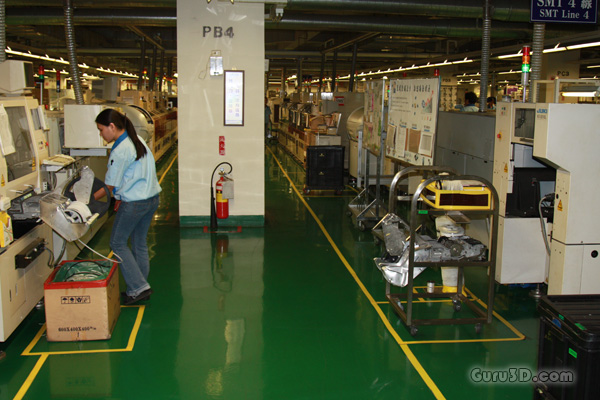
But let's start at stage one, we enter the SMT hall. Here we can see one production line. Try to look and see how deep these lines go. If you look to the left you'll spot a manufacturing run of a motherboard.
You see very few people here because the fabrication process is as autonomous as it can be from beginning to end. That's something else at the DIP stage alright. But more on that later, of course.

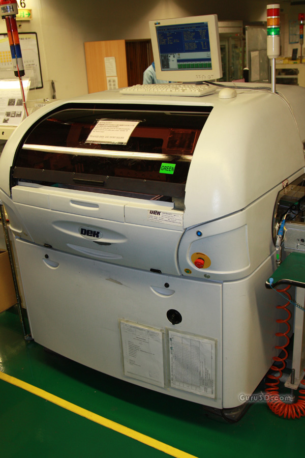
So the first step in product development is then what is called the SMT stage. Above a DEK Infinity solder paste screen printer.
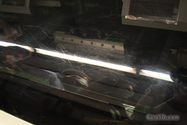
The SMT machinery gives the clear PCB a solder print job before they apply them with surface-mounted components like resistors, capacitors etc. (all the really small stuff). So this is the actual solder paste printer. Let's try and see though the safety glass.

Now it is horribly hard to see what is going on here. But this is the first step. Traced empty PCBs are inserted into this machine where they will get a layer of conductive solder. The solder paste is distributed over the screen by the printer so it is squeezed through the actual holes in a nickel sheet to adhere to the motherboard underneath in very specific and precise areas.

With the solder paste applied in the proper positions, the next step is to mount all the tiny stuff like resistors, voltage regulators, small capacitors etc.. This is where this process gets its name from, SMT (Surface Mount Technology).
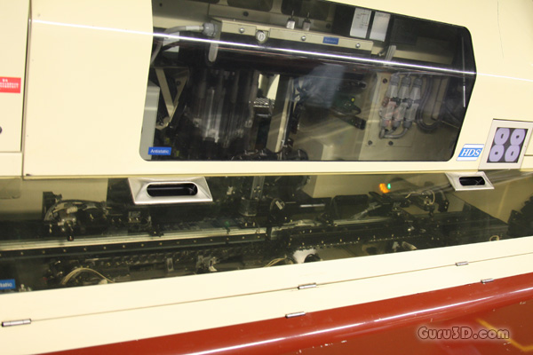
What you see is a machine with a component gun, using a FUJI CP742 high speed SMT machine. This machine will add components like tiny resistors up to the North and Southbridge chips. You have no idea how fast this machine really is, if I recall it right, it does each component process mount within merely an eighth of a second per component.
