The GPU that makes it happen ... GF104
The GPU that makes it happen ... GF104
 So then, the GeForce GTX 460. Typically we dive deeply into the graphics core architecture. For this article, being very lengthy, I would like to keep things a little bit more simple and easy to grasp -- to keep things understandable.
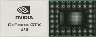
The GeForce GTX 460 series is to be based on a new chip, initially the Fermi architecture you all have seen on the GTX 465, 470 and 480 is based on the GF100 chip. The Mid-range GeForce GTX 460 is still based on that Fermi architecture, yet for this round NVIDIA designed a new chip, so this is not a GF100 with disabled Shader clusters. Make no mistake here, the architecture is still based on Fermi, same setup, same caches, yet now a much smaller chip with less transistors (2.1 Billion to be precise), called the GF104. GF104 is a less complicated chip to manufacture as the smaller transistor count directly relates to better yields, heat levels, better voltages and thus a better TDP as well. It is a smaller chip to produce.
For this round NVIDIA will put the GF104 chip onto two products, the GeForce GTX 460 with 768MB of graphics memory and the GeForce GTX 460 with 1024MB of memory. For the bigger part of the specification the two are similar when it comes to shader processor count, memory bus and clock frequencies, the 1GB model however definitely will be a good chunk faster, as cutting away 256MB of memory also cuts away a chunk of the ROP engine.
So you might wonder, why two models? Well, initially we felt that the 768MB version would end up in OEM mostly, then again, at sub-200 USD this card surprised us as it offers a lot of bang for buck alright. Who knows, time will tell which model will sell the best. Regardless of its 768MB of memory, as we'll demonstrate it is a sexy performer in the mid-range for sure.
Yes, performance wise these cards will be really interesting. But we'd almost forget that the GeForce GTX 460 cards will be fully fledged DirectX 11 class cards with nice tessellation performance and the full DX11 API feature set. Though only a handful of games really show significant DX11 class quality, we really feel that if you are in the market for a new graphics card, DX11 is obviously the path to follow.
Should you not yet be familiar with DirectX 11 and stuff like shaders and Tessellation, we'll explain all that in our standard skinny of content over the next few pages as well, don't worry... this is Guru3D.com and we explain everything as much as we can in understandable wording and terms. Let's compare some of the specs to the GeForce GTX 465, which we really think will go EOL real fast, real soon, as the GTX 460 cards are equally fast and often even faster due to all OC edition SKUs.
Reference specifications:
| Graphics card | GeForce GTX 460 768MB | GeForce GTX 460 1024MB | GeForce GTX 465 1024MB |
| Graphics Processing Clusters | 2 | 2 | 3 |
| Streaming Multiprocessors | 7 | 7 | 11 |
| Shader processor | 336 | 336 | 352 |
| Texture Units | 56 | 56 | 44 |
| ROPs | 24 | 32 | 32 |
| Core Clock | 675 MHz | 675 MHz | 607 MHz |
| Shader Clock | 1350 MHz | 1350 MHz | 1215 MHz |
| Memory Data rate | 3600 MHz | 3600 MHz | 3200 MHz |
| Graphics Memory | 768MB GDDR5 | 1024MB GDDR5 | 1024MB GDDR5 |
| Memory interface | 192-bit | 256-bit | 256-bit |
| Memory bandwidth | 86.4 GB/s | 115.2 GB/s | 102.6 GB/S |
| Texture Fillrate Bilinear | 37.8 GigaTexels/sec | 37.8 GigaTexels/sec | 26.7 GigaTexels/sec |
| Fab node | 40nm | 40nm | 40nm |
| TDP | 150 Watts | 160 Watts | 200 Watts |

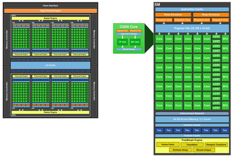
If you look closely at the SM partitions, then you can see and calculate that the 336 Shader processors based GF104 in fact has eight SM partitions. 7 are enabled = 336 Shader processors. Burt expect another SKU in the future as well as that GPU really has 384 shader processors.
Okay, so back to the two reference SKUs, let me break them down real simple:
- GeForce GTX 460 768MB - 336 Shader processor - 56 TMUs - 24 ROPs - TDP 22/150W - MSRP 199 USD
- GeForce GTX 460 1024MB -336 Shader processor - 56 TMUs - 32 ROPs - TDP 22/160W - MSRP 229 USD
So, both cards in reference setup will be clocked at 675 MHz on the core frequency, and in NVIDIA's typical 1:2 setup mode 1350 MHz on the 336 shader processors. There will be a lot of overclocking headroom on these boards as 800 MHz should not be an issue (even without voltage tweaking). The gDDR5 memory will be clocked at a slightly shy 3.6 Gbps which is 3600MHz effective (quad data rate). The 768MB version then will make use of three 64-bit memory controllers which boils down to 192-bit memory, and the 1024 GB model has one extra cluster of 256MB attached to it, which requires one more 64-bit memory controller and this one operates at 256-bit memory bus width.

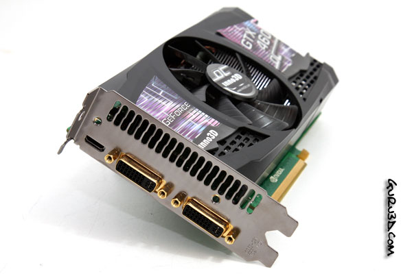
Above, the Inno3D OC design. The cards are based on a dual-slot cooling design and come with two gold-plated dual-link DVI and a HDMI connector. HDMI will again pass through sound including bit streaming support for Dolby True HD and DTS-HD Master. Being a mid-range product, only 2-way SLI will be allowed and thus you'll only see a single SLI finger/connector on the PCBs. Okay, the next stop will be an extensive photo-shoot.
