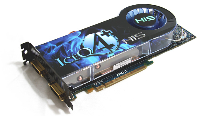
What's hidden under the VGA cooler ?
What's hidden under the VGA cooler?
As you guys know by now ATI's Radeon HD 4850/4870 both use the same GPU (graphics processor). The codename for these chips is RV770. AMD put nearly a billion transistors into that GPU, which is now built upon a 55nm (260 mm2 Die size) production. The chip literally is 16 mm wide and high. Which for AMD still is quite large, for a 55nm product. The number of transistors for a midrange product like this is extreme and typically it's best to directly relate that to the number of shader processors to get a better understanding. But first let's look at some nice examples of Die sizes of current architectures.
The Radeon 4850/4870 series graphics processors have 800 scalar processors (320 on the HD 3800 series) and now have a significant forty texture units (was 16 in last-gen architecture). The stream/compute/shader processors (can we please just name them all shader processors?) definitely had a good number of changes; if you are into this geek talk, you'll spot 10 SIMD clusters each carrying 80 32-bit Shader processors (this accumulates to 800). If I remember correctly, one SIMD unit can handle double precision.
Much like we recently noticed in the NVIDIA GTX 200 architecture, the 80 scalar stream processors per SIMD unit have 16KB of local data cache/buffer that is shared among the shader processors. Next to the hefty shader processor increase you probably already notice the massive amount of texture units. In the last generation product we noticed 16 units, the 4800 series has 40 units.
When you do some quick math, that's 2.5x the number of shader processors over the last-gen product, and 2.5x the number of texture units. That's a pretty grand change folks. Since the GPU has 800 shader processors it can produce the raw power of 1000 to 1200 GFlops in simple precision. It's a bit lame and inaccurate to do but divide the number of ATI's scalar shader processors with the number 5 and you'll roughly equal the performance to NVIDIA's stream processor. You could (in an abstract way) say that the 4800 series have 160 Shader units, if that helps you compare it towards NVIDIA's scaling. Again there's nothing scientific or objective about that explanation.
Effectively combined with the clock speed and memory this product can poop out 1000/1200 GigaFLOPs of performance. Depending on how that is measured of course. But still, with an entry product at 199 USD for the 4850 and 299 USD for the 4870 that's just an awful lot of computing power.
Let's compile a chart of the reference specifications:
|
|
ATI Radeon |
ATI Radeon |
ATI Radeon |
ATI Radeon |
|
# of transistors |
965 million |
965 million |
666 million |
965 million |
|
Stream Processing Units |
800 |
800 |
320 |
800 |
|
Clock speed |
625 MHz |
625 MHz |
670 MHz |
750 MHz |
|
Memory Clock |
2000 MHz GDDR3 (effective) |
1980 MHz GDDR3 (effective) |
1.66 GHz GDDR3 (effective) |
3600 MHz GDDR5 (effective) |
|
Math processing rate (Multiply Add) |
1000 GigaFLOPS |
1200 GigaFLOPS |
428 GigaFLOPS |
1200 GigaFLOPS |
|
Texture Units |
40 |
40 |
16 |
40 |
|
Render back-ends |
16 |
16 |
16 |
16 |
|
Memory |
512MB GDDR3 |
512MB GDDR3 |
512MB GDDR3 |
512MB1024/ GDDR5 |
|
Memory interface |
256-bit |
256-bit |
256-bit |
256-bit |
|
Fabrication process |
55nm |
55nm |
55nm |
55nm |
|
Power Consumption (peak) |
~110W |
~110W |
~90W |
~160W |

