The Graphics engine architecture
The Graphics engine architecture
So I kept the more complex stuff for last in the technology overview. If this seems a little too techy for you, skip this page please.
AMD is moving away from the VLIW5 and VLIW4 architecture we have seen in the last generation of products. If anything, VLIW4 has shown certain inefficiencies in the Radeon HD 6900 series and while VLIW designs are fine for graphics they are not so grand for computing.
The new graphics core architecture is now marketed as GCN, which is short for Graphics Core Next architecture and the architecture building block has changed significantly to remove certain inefficiencies seen in the VLIW architecture.
A GCN in its essence is the basis of a GPU that performs well at both graphical and computing tasks. For the compute side of things the new GCN Compute unit model has been introduced, it is designed for better utilization, high throughput and multi tasking. E.g. performance, performance, performance.

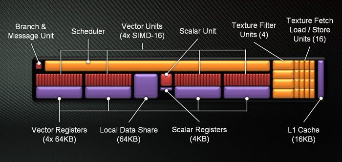
So your basic new Shader cluster is one called a (GCN) Compute Unit:
- Non-VLIW Design
- 16 wide SIMD Units
- 64 KB registers / SIMD Unit
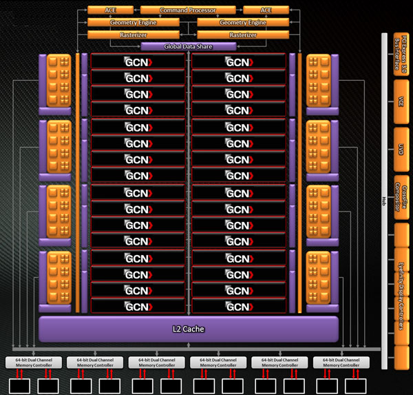
Now if we take 4 of these SIMD Units, that will form the basis of one Compute Unit (CU). Each SIMD unit is 16 wide, times four per compute unit means that each CU unit has 64 shader processors. The GPU has 32 Compute units meaning 64SIMDs x 32 CUs = 2048 Shader processors (for the R7970).
- Engine has Dual Geometry engines / Asynchronous Compute engines
- 8 render backends / 32 color ROPs per clock cycle / 128 Z/Stencil ROPs per clock
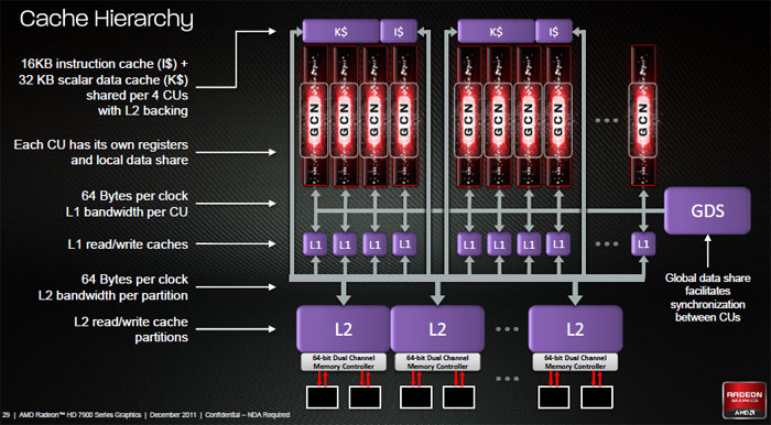
- Engine ties to 768KB R/W L2 cache
- Tahiti GPU has up-to 32 Compute Units
The Graphics Core Next Compute Unit (CU) has about the same floating point power per clock as the previous one (i.e. Cayman). It also has the same amount of register space (for the vector units). Each CU also has it's own registers and local data share.

Again: one compute unit just as a Cayman SIMD is a collection of shader processors, four SIMDs form one compute unit. Caymans (6900) problem was that it was not so efficient with multiple tasks at once.
Cayman had/has 16 4-wide VLIW processing elements for a total of 16x4=64 operations in parallel, while the new architecture has 4 16-wide vector processors, again for a total of 4x16=64 operations per clock. GCN also has a scalar processor that Cayman does not.
The distinction is in its bare essence that GCN does not need instruction level parallelism, each of the four 16-wide SIMD vector units execute a different wavefront being the whole 64-sized wavefront taking four cycles.

So the theoretical floating point power stays more or less the same per CU, but GCN will be more efficient since it does not require instruction level parallelism (we assume it costs some more area/transistors as well). The outcome, compiling also becomes much more uncomplicated and that means more efficiency and thus there it is again, better performance.
GCN is all about creating a GPU good for both graphics and computing purposes. Oh and all compute units ... combined with the other ASIC components form the GPU. See, easy peasy right :)
