The Product Specifications
The Product Specifications
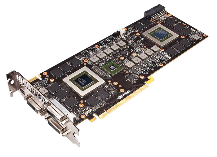
So the GeForce GTX 690 in very short wording is one graphics card made out of two graphics processors. Two become one, it's really as simple as I can put it. Internally these two GPUs are connected through a PCIe connection (PLX) and they then operate in SLI mode. To accomplish something really sturdy and powerful, NVIDIA took their fastest (currently) GPUs available and without any compromises on the number of shader processors etc. inside that GPU they started designing the card.
The end result is a dual-GPU product that runs two ICs called and tagged the GK104, these are the very same GPUs you'll find on the GeForce GTX 680, and in it's bare essence the GTX 690 is in fact two 680s clocked marginally slower.

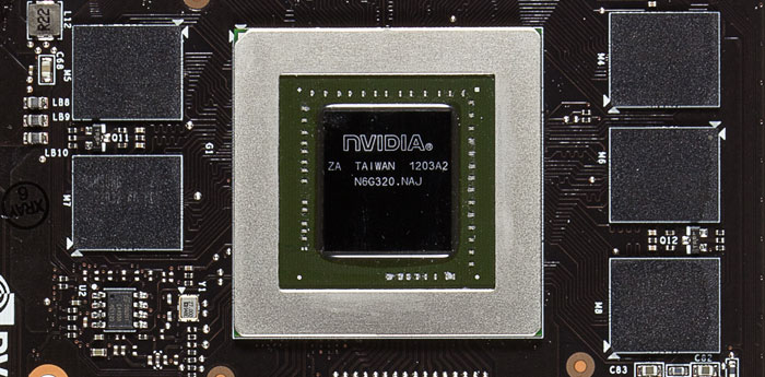
Expanding it a little -- that's two GK104 GPUs (shown above) on a single graphics card connected through a PLX PCIe Gen 3 bridge chip with a total of 3072 Shader processors (2 x 1536) for both GPUs and 4 GB of GDDR5 memory (2GB per GPU), all that on a 10-layer PCB. The GPUs get 10 power phases. Cooling wise NVIDIA extends the usage of vapor-chamber cooling.
The new Dual-GPU solution is of course DirectX 11 ready. The product is obviously PCI-Express 3.0 ready and has a maximum board power of around 300W with a typical draw of 260~265 Watts.
As far as the memory specs of the GK104 Kepler GPU are concerned, the boards will feature a 256-bit memory bus connected to 2 GB of GDDR5 video buffer memory per GPU. The reference memory clock is set at 6 GHz / Gbps (effective), similar to the GTX 680. This boils down to a memory bandwidth of 192 GB/s on that 256-bit memory bus (per GPU).
An immediate difference to the GPU core versus the shader processor domain is that both will be clocked at 1:1, meaning both the core and shader domain clock in at 915 MHz, that means the 2x shader hotclock from the last generation products is a thing of the past.
New however is a boost (turbo) clock set at 1019 MHz, we'll explain this later on.
| GeForce GTX 285 |
GeForce GTX 480 |
GeForce GTX 580 |
GeForce GTX 590 |
GeForce GTX 680 |
GeForce GTX 690 | |
| Stream (Shader) Processors | 240 | 480 | 512 | 1024 | 1536 | 3072 |
| Core Clock (MHz) | 648 | 700 | 772 | 607 | 1006 | 915 |
| Shader Clock (MHz) | 1476 | 1400 | 1544 | 1215 | - | - |
| Boost clock (Mhz) | - | - | - | - | 1058 | 1019 |
| Memory Clock (effective MHz) | 2400 | 3700 | 4000 | 3414 | 6000 | 6000 |
| Memory amount | 1024 MB | 1536 | 1536 | 3072 | 2048 | 4096 |
| Memory Interface | 512-bit | 384-bit | 384-bit | 384-bit | 256-bit | 256-bit |
| Memory Type | GDDR3 | GDDR5 | GDDR5 | GDDR5 | GDDR5 | GDDR5 |
Memory wise NVIDIA has sizable and expensive memory volumes due to their architecture, we pass 1 GB per GPU as standard these days for most of NVIDIA's series 500/600 graphics cards. Where the dual-GPU GeForce GTX 590 had 3072 MB of GDDR5 memory the GeForce GTX 690 has 4096 MB of GDDR5 memory.
As you can understand, the memory partitions, bus-width and combination of GDDR5 memory (quad data rate) allow the GPU to work with a higher and much needed framebuffer bandwidth (effective). Let's put more data in a chart to get an idea and overview of some specific changes:
| Graphics card | GeForce GTX 580 | GeForce GTX 590 | GeForce GTX 680 | GeForce GTX 690 |
| Fabrication node | 40nm | 40nm | 28nm | 28nm |
| Shader processors | 512 | 1024 | 1536 | 3072 |
| Streaming Multiprocessors (SM) | 16 | 32 | 8 | 16 |
| Texture Units | 64 | 128 | 128 | 128x2 |
| ROP units | 48 | 96 | 32 | 32x2 |
| Graphics Clock (Core) | 772 MHz | 607 MHz | 1006/1058MHz | 915/1019MHz |
| Shader Processor Clock | 1544 MHz | 1215 MHz | 1006/1058MHz | 915/1019MHz |
| Memory Clock / Data rate MHz | 1000 / 4000 | 854 / 3414 | 1502 / 6008 MHz | 1502 / 6008 MHz |
| Graphics memory | 1536 MB | 3072 MB | 2048 MB | 4096 MB |
| Memory interface | 384-bit | 384-bit | 256-bit | 256-bit |
| Memory bandwidth | 192 GB/s | 164 GB/s per GPU | 192 GB/s | 192 GB/s |
| Power connectors | 1x6-pin PEG, 1x8-pin PEG | 2x8-pin PEG | 1x6-pin PEG, 1x8-pin | 2x8-pin PEG |
| Max board power (TDP) | 244 Watts | 365 Watts | 170 Watts | 300 Watts |
| Recommended Power supply | 600 Watts | 700 Watts | 550 Watts | 750 Watts |
| GPU Thermal Threshold | 97 degrees C | 97 degrees C | 98 degrees C | 98 degrees C |
The TDP is roughly 300 Watts, a very respectable number really. TDP = Thermal Design Power. Roughly translated, when you stress everything on the graphics card 100%, your maximum power consumption is the TDP. During overall gaming the power consumption will be lower.
The GeForce GTX 690 comes with both two 8-pin power connectors to get enough current and still have some for overclocking.

