Power efficiency - Dyn Clock Adjustment
Power efficiency
Moving towards a 28nm based chip means you can do more with less as the product becomes smaller, the GK104 GPU comes with roughly 3.54 billion transistors embedded into it. The TDP (maximum board power) sits at a very respectable 170 Watts. So in one hand you have a graphics card that uses less power, yet offers more performance. That's always a big win!
The GeForce GTX 670 comes with two 6-pin power connectors to get enough current and a little spare for overclocking. This boils down as: 2x 6-pin PEG = 150W + PCIe slot = 75W is 225W available (in theory). We'll measure all that later on in the article but directly related is the following chapter.
Dynamic Clock Adjustment technology
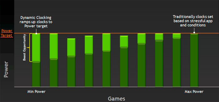
Kepler GPU will feature a Dynamic Clock Adjustment technology and we can explain it easily without any complexity.
Typically when your graphics card idles the cards clock frequency will go down... yes? Well, obviously Kepler architecture cards will do this as well, yet now it works vice versa as well. If in a game the GPU has room left for some more, it will increase the clock frequency a little and add some extra performance. You could say that the graphics card is maximizing it's available power threshold.

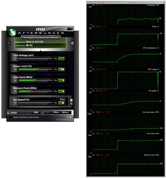
Even more simple, DCA resembles Intels Turbo Boost technology a little bit by automatically increasing the graphics core frequency with 5 to 10 percent when the card works bellow its rated TDP. The baseclock of the GTX 670 in 3D mode is 915 MHz, it can now boost towards 980 MHz or even higher when the power envelope allows it to do so. The "Boost Clock" however is directly related to the maximum board power, so it might clock even higher as longs as the GPU sticks within it's power target. We've seen the GPU run to an excess of even over 1080 MHz for brief periods of time.
Overclocking on that end will work the same as GPU boost will continue to work while overclocking, it stays restricted within the TDP bracket. We'll show you that in out overclocking chapter.

