The Haswell Architecture
Haswell Architecture, A Little Deeper...
Ivy Bridge was all about transitioning towards a new, smaller fabrication process. Whereas Clarkdale (Core i5-661 etc.) processors had a 45 nm GPU (sounds ancient , I know!) and a 32 nm CPU core placed onto one chip package, Sandy Bridge (Core i7-2600 etc.) architecture came together and merged these two parts on the die, all based on a 32 nm fabrication node. That was the concept for IB as well, but now the fabrication process for Ivy Bridge is 22 nm. It's the same for Haswell, the Core i7 based processors will have four physical (execution) CPU cores each capable of one hyper-thread (making 4 physical cores and 8 logical cores hyper-threaded), they include integrated graphics (4000 series which we'll discuss in a minute) and a memory controller. Like other 1st generation Nehalem derivatives, Haswell will feature Intel Turbo Boost. The 4th generation processors there will of course be a distinction per processor segment (i3/i5/i7). What you get in terms of features and what you need to remember limitation wise:
- Desktop Core i7 processors have four cores / eight hyper-threads / Up to 8 MB L3 cache
- Desktop Core i5 processors have four cores / NO hyper-threading / Up to 6 MB L3 cache
- Desktop Core i3 processors have two cores
All models will come with the latest revision turbo mode but only the Core i7 series will be capable of handling multiple independent software threads per core, also known as hyper-threading. It's a feature we like very much as it really helps out on peak performance by allowing a processor to execute two different code streams at pretty much the same time.
The Core i7 Haswell processors feature 8 MB of Intel Smart Cache (the L3 cache) and an Integrated Memory Controller (IMC) that supports two-channels of DDR3 memory at officially supported speeds of 1333/1600 MHz (but can do much higher). We've seen memory and motherboard partners advertise close to 3 GHz on the DDR3 memory).
Core i5 and i3 will have smaller L3 caches of 6 MB. For the performance-mongers amongst us the 4790(K) and 4690(K) models, the most interesting for an easy overclock are the K models. But let's have a look at the die photos. First Sandy Bridge, then Ivy Bridge.
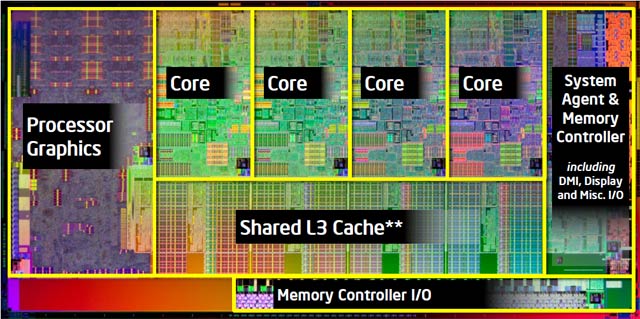
Above, Sandy Bridge Architecture
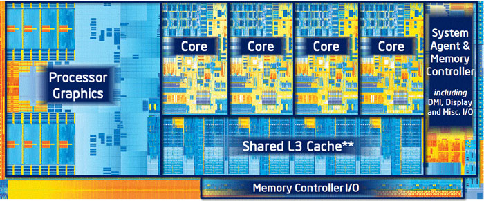
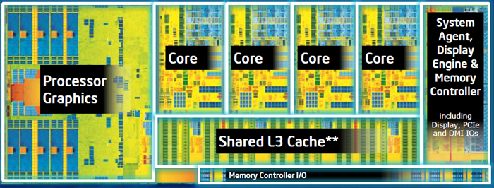
Above, Ivy Bridge Architecture
Above, Haswell Architecture
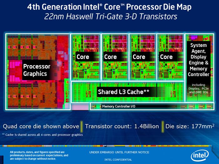
As you can see it's a very similar architecture, Sandy Bridge was the building block for Ivy Bridge and Ivy Bridge is the building block for Haswell, definitely something that you can see is that the CPU units have changed a bit. If you go a little deeper into the core then your first question will be, what about L1 and L2 caches? The Haswell cache memory consists of a 32 KB L1 Data cache, 32 KB Instruction cache (= 64 KB L1) and then we spot a 256 KB L2 cache per core. Load bandwith however has doubled up from 32 to 64 Bytes per cycle and the store bandwith from 16 to 32 Bytes per cycle. So the the L1 data cache in Haswell is the same size and latency, but with a third more bandwidth.
Then there's a nice L3 cache that is shared in-between the CPU cores which is 8 MB in total for the Core i7 47xx processors and 6 MB for the Core i5-45xx. The L3 cache is where the magic happens, surrounded by the segments inside the die, the L3 cache sits in the physical form of a ringbus. Thus the L3 cache can be used by the processor cores and also the graphics core.
