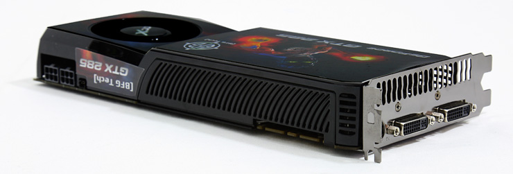
The GeForce GTX 285 GPU
The GeForce GTX 285 GPU
So the GTX 285 is all about the 55nm fabrication based product series GTX 200. The GTX series 200 GPUs amounts up to 1400 million transistors. It's the biggest goblin of a graphics processor that NVIDIA has ever built with 1400 million transistors. 1400 million transistors, if you think about that for a minute you might go nuts. Keep in mind that one of the best GPUs ever made, the GeForce 8800 'only' had around 700 Million transistors. It makes much sense for NVIDIA to get that die size down as they were still stuck on an architecture based on 65nm as fabricated by TSMC.
GeForce GTX 285
- 1.4 billion transistors
- 993 GigaFLOP processing power
- 240 processing (shader) cores (GTX 280)
- 55nm node fabrication
- DirectX 10
- New power management enhancements
- CUDA parallel processing
- GeForce PhysX
How different is the GTX 280 to the GTX 285? A very valid question, the answer is: for you as an end user, not much. Aside from some small clock frequency changes and a minor performance increase it is 99% the same product. The GeForce GTX 285 still has 240 stream processors.
The new GeForce GTX 285 will run at a core clock frequency of 648 MHz. There are more clocked domains inside that GPU though, the shader processor run at 1496 MHz and the memory is at 1242 MHz (effective 2484 MHz). And though that is a higher clock opposed to the previous GTX 280, it accounts for only a little extra performance.
| GeForce 9800 GTX |
GeForce GTX 260 |
GeForce GTX 280 |
GeForce GTX 285 |
GeForce GTX 295 | |
| Stream (Shader) Processors | 128 | 192 | 240 | 240 | 240 x2 |
| Core Clock (MHz) | 675 | 576 | 602 | 648 | 576 |
| Shader Clock (MHz) | 1675 | 1242 | 1296 | 1476 | 1242 |
| Memory Clock (MHz) x2 | 1100 | 999 | 1053 | 1242 | 999 |
| Memory amount | 512 MB | 896 MB | 1024 MB | 1024 MB | 1792 MB |
| Memory Interface | 256-bit | 448-bit | 512-bit | 512-bit | 448-bit x2 |
| HDCP | Yes | Yes | Yes | Yes | Yes |
| Two Dual link DVI | Yes | Yes | Yes | Yes | Yes |
For the folks that like to go a little deeper: this high-end part has 1GB of GDDR3 memory which has a 512-bit memory bus that binds to 8 memory controllers inside the GPU. At the end of the pipeline we run into an improved ROP (Raster Operation) engine, and the 280 has 32 of them and 80 texture filtering units. Performance accounts up to roughly 1 TFLOP (depending how you measure it actually), so the new clocks bring NVIDIA to the missed Teraflop from the GTX 280 launch...
What's great about its release is that a move towards a smaller die and fabrication process (55nm) often brings several advantages. The new GTX 285 part requires a little less voltage, as a result it consumes less power. And a result of that is that this card no longer needs both the 6-pin and 8-pin power connectors to get enough juice. You'll spot two 6-pin connectors on the boards.
The TDP (peak wattage) is now roughly 183 Watts (GTX 280 = 235W), which in all honesty is extremely good. See, the product got faster, yet consumes less power. That's a win in my book.
Cast your mind back to the GeForce 8800 Ultra which isn't that far off from that 235W peak either. The GTX 285 is much faster. So the performance per Watt again has increased on many fronts.
So again, the power for the GTX 285 is fed by two six-pin connectors. Power consumption for this 10.5-inch board is 183W.

