Threadripper Generation 3 and TRX40
Threadripper Generation 3 and the TRX40 platform
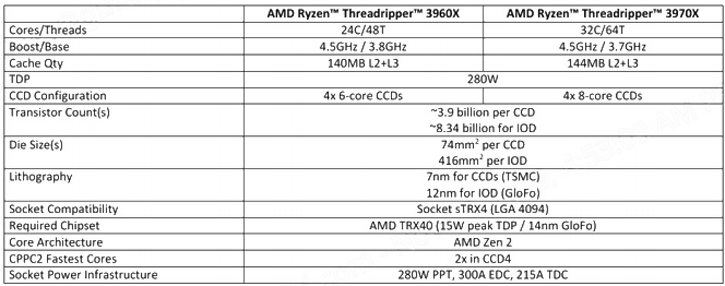
Before we start the photoshoot, first an overview of the new processors and the new platform. Threadripper processors are CPUs based upon Ryzen architecture dies that you know from the 'regular' Ryzen 3000 series processors. While a lot of IO changes have been made to facilitate it, basically on-chip you'll spot four 8-core Ryzen processor dies sitting around a big IO chip, all in one package This means these processors are set up in a 8+8+8+8 (4x8) fashion for the 32 core 3970X, with disabled cores for the other SKUs. The 3960X processor has 24 active cores, that means it will be set up as 6+6+6+6, and AMD activated the fastest working cores for you. The processor dies are physically similar to the 8-core Ryzen 3000 / ZEN2 design, it is the very same die that is used, however, binned for best-performing cores at the lowest possible voltage. Zen 2 architecture is an advancement of Zen, and Zen had some bottlenecks that needed to be dealt with. These are solved in this design and, at the same time, thanks to the smaller 7nm transistors, added extra functionality in important places. There are differences between the three cache levels. The L1 instruction cache has become smaller at 32 Kbytes, the data cache is the same as last gen, 32 Kbytes, both per-core of course.
The L2 cache is also the same at 512Kbytes per core, however, the L3 cache was doubled up from last gen moving from 8Mbyte towards 16 Mbyte per CCX (core complex). So that's 128 MB in total. So in retrospect, AMD reduced the L1 instruction cache from 64 kB to 32 kB. The instruction cache contains the x86 instructions that are retrieved from the memory for processing. However, by giving this cache more inputs and outputs, 8-way associative instead of 4-way associative, it will make up for that design choice. Also, by optimizing algorithms for pre-fetching instructions and increasing the caches at other levels (like the L3 cache), the effect of the smaller instruction cache is limited. The L1 data cache was 32 kB in Zen and remains at 32 kB for Zen 2. Unchanged is the L2 cache, which is still 512 kB per core. The L3 cache, however, is shared by the cores and that one has doubled up in size. Four cores are partitioned together in a group called a core complex (CCX). The earlier generation Zen processors had 8 MB of L3 cache, this has been doubled up to a whopping 16 MB of L3 cache. Why the double L3 cache? Well, AMD needed to address the latencies for accessing working memory to cope with the chiplet design, whereby the memory controller is physically located in a different chip, ergo a doubled L3 cache. Increasing any sort of cache is costly. It takes up a substantial portion of the available transistor budget, here is where 7nm helps out greatly.
Chiplet design
Starting at Zen 2 architecture AMD moved towards a chiplet design. Multi-die chips holding their CPU cores are paired with multiple chips in one package. So, for Threadripper 3000, that would be four processor dies interconnected by an IO chip, that IO chip is similar to the chipset IC. It’s one of the many answers to be able to fight off Moore's Law, now and in the future. AMD was already using the technology to connect multiple processors in Threadripper and, for servers, Epyc. Actually, also Intel with Kaby Lake-G. Chiplets, are multiples of chips put together on an interposer that forms the actual chip. Chiplets with Zen 2 feature a I/O die along with 7nm CPU chiplets (each holding eight cores per die). To be able to accomplish that, AMD has been updating its Infinity Fabric that connects the different dies that hold the cores. Current Epyc, Ryzen and Threadripper CPUs are all connected via the Infinity Fabric. With the Zen 2 architecture, AMD places one I/O die chip that sits in the middle, which is connected to four 8-core dies and, with the 64-core part, a staggering eight 8-core dies. These AMD CPU chiplets are connected through Infinity Fabric (the interlink wires that connect them all). Why chiplet designs? One of the bigger issues at hand when manufacturing large monolithic CPU/GPU dies is that yields decrease nearly exponentially and costs go up due to non-working dies. Multiple smaller chips in one package have higher yields, less loss and thus can be more profitable.
The Ryzen Threadripper processor family
On the market, you will spot Ryzen series 3000 3, 5, 7, 9 and now Threadripper series 3000 processors based on ZEN2 architecture. It’s plain and simple and, as always, that works out as the best way to understand the product positioning. Below, an overview of the Threadripper lineup.
You'll notice the 3990X, this is confirmed for a 2020 launch. Given its numbering and knowing AMD (albeit unconfirmed) we do expect a 48-core part as well.
Chipset: T-REX
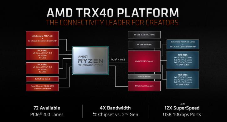
A new chipset has been born. TRX40 is specifically for Threadripper 3000 and future products. It was imperative for AMD to get the most out of Threadripper 3000 and thus they wanted to double up the PCIe Gen 4.0 interlink between the processor and motherboard chipset. This chipset has a PCIe 4.0 x8 interlink, which is unheard of and creates massive possibilities for things like storage. So, that bandwidth between the processor and the chipset has quadrupled compared to the current Threadripper platform. As a result, much more bandwidth is available for all I/O options offered by the chipset. What you are also going to notice is a further increase in PCIe Gen4 lanes, 72 available lanes on the Threadripper 3000 platform. Threadripper 3000 brings 64 PCIe Gen4 lanes to the table, 8 of those have been reserved for the chipset link and then the chipset link brings in another 24 PCIe Gen 4 links to the table with 8 reserved for that interconnect. In total, you are looking at 88 lanes, with 72 lanes available to the end-user. The socket has been named sTRX4. You are going to see a number of motherboard announcements today, the new Threadripper processors and platforms will become available by the 25th of November. So yes, PCIe Gen 4.0 everywhere. The socket has been named sTRX4, the chipset TRX40.
| PCIe Version | Line Code | Transfer Rate | x1 Bandwidth | x4 | x8 | x16 |
|---|---|---|---|---|---|---|
| 1.0 | 8b/10b | 2.5 GT/s | 250 MB/s | 1 GB/s | 2 GB/s | 4 GB/s |
| 2.0 | 8b/10b | 5 GT/s | 500 MB/s | 2 GB/s | 4 GB/s | 8 GB/s |
| 3.0 | 128b/130b | 8 GT/s | 984.6 MB/s | 3.938 GB/s | 7.877 GB/s | 15.754 GB/s |
| 4.0 | 128b/130b | 16 GT/s | 1.969 GB/s | 7.877 GB/s | 15.754 GB/s | 31.508 GB/s |
Quad-channel DDR4 memory
AMD’s DDR4 support is good these days and with Zen 2 it has become great - pretty much all brands are supported, with an increase in frequency support as well as a drop in latency. Obviously you get quad-channel memory support with the slowest default rating at 3200 MHz / 3200MT/s (JEDEC). Much like Ryzen 3000, a 2:1 multiplier switches on at DDR4-3733 or higher frequencies so do keep in mind that it will have an effect on the speed at which the various core complexes within the CPU can communicate with each other. For the memory itself it can now hold 128 GB with 4x8 Single Rank supported out of the box at 3200 MHz. Of course, the memory used in real practice can go faster, in fact, we'll be using a 64GB 3600 MHz CL16 kit from Corsair (Dominator) on the platform. You can even go 256GB in an 8x32 Dual Rank configuration, here however the JEDEC spec drops to 2667 MHz.
| Memory config | Rank | Official JEDEC frequency support |
| 4x8 | Single | DDR4-3200 |
| 8x8 | Single | DDR4-2933 |
| 4x16 | Dual | DDR4-3200 |
| 8x16 | Dual | DDR4-2667 |
| 4x32 | Dual | DDR4-3200 |
| 8x32 | Dual | DDR4-2667 |
What's the difference between Single and Dual Rank memory is a question we receive often. Speaking in theory, Single Rank memory is faster than Dual Rank memory; when a computer accesses Single Rank memory, explained extremely simply, it means it only has to go around 'its' track once, whereas with Dual Rank it would have to go around the track twice as it is a separated circuit. See it as two DDR4 DIMMs on one DIMM PCB.
- A Single Rank DIMM has one set of memory chips that is accessed while writing to or reading from the memory. A Dual Rank DIMM is similar to having two Single Rank DIMMs on the same module, with only one rank accessible at a time. There's also a Quad Rank DIMM these days, effectively, two Dual Rank DIMMs on the same module. Only one rank is accessible at a time.
- Dual and Quad Rank DIMMs provide the greatest capacity with the existing memory technology. For example, if current DRAM technology supports 8 GB Single Rank DIMMs, a Dual Rank DIMM would be 16 GB, and a Quad Rank DIMM would be 32 GB.
The main idea behind memory ranking - to cram more memory into a single-slot module, decreasing the number of banks needed. Ranks have more to do with density and pricing than actual performance. Obviously, always check with your mainboard manufacturer if the DDR4 modules are supported, they often offer a QVL list. Also, ECC DDR4 is supported on the Threadripper platform.


