Intel Launches Core i7-2700K Processor

Processor 721 Published by Hilbert Hagedoorn 0

Well it was expected for a while now, Intel released its latest performance-segment processor, the Core i7-2700K. The i7-2700K is a quad-core chip in the LGA1155 package, based on the 32 nm "Sandy Bridge" silicon. It is clocked at 3.50 GHz, and features an unlocked base clock ratio multiplier, which makes overclocking possible. It features AVX instruction set, AES native acceleration, HyperThreading (which enables 8 logical CPUs), 256 KB L2 cache per core, and 8 MB of shared L3 cache.

Apart from these, it packs a dual-channel DDR3 integrated memory controller, PCI-Express root complex, and Intel HD 3000 series integrated graphics. The TDP remains consistent with many other Core i5 and Core i7 "Sandy Bridge" chips, at 95W. An interesting development here is that the pricing of Core i7-2700K didn't turn out to be what Amazon and MWave were charging for their pre-orders (around US $380), the retail price of this chip is merely $15 higher than that of the Core i7-2600K, at $332.


» Read full story

Intel Retailers Raise CPU Prices After Bulldozer Launch

Processor 721 Published by Hilbert Hagedoorn 0

The performance bracket that AMD's FX-Series desktop processors are delivering, apparently made Intel reconsider the prices of its Core i5 and Core i7 processors, which now seem to retail for higher prices than before Bulldozer was out.

Intel has seen AMD's inability to deliver a hefty competing product as an opportunity to increase the margins of its products.

Using the Geizhals.at price comparison engines, one of the largest of its kind in the world, Bright Side of News analyzed the prices of Intel's processors both before and after the launch of AMD's FX-Series CPUs.

This way, the Website has found out that pricing for the Core i7-2600K rose from


» Read full story

Intel Core i7-3930K and Core i7-3960X Listed in EU

Processor 721 Published by Hilbert Hagedoorn 0

With a little less than a month to go until Intel will make official its first processors based on the high-performance Sandy Bridge-E architecture, European retailers have started listing some of these chips on their websites, the Core i7-3930K and Core i7-3960X being the first to arrive.

These two Intel processors have popped up in Sweden on the PriceSpy website. After dropping the 25% VAT tax from the price of these CPUs, it would result that the Core i7-3960X is priced at $1086 US, or about 786 Euros, while its slower brother has a retail price of $616 US (446 Euros).

Both of these prices are higher than those suggested by previous leaks, $999 and $583 respectively, but they are expected to come down once we are getting nearer to the Sandy Bridge-E release date.

Intel's initial LGA 2011 processor lineup will include three chips, all of them belonging to the Core i7 product line.

As most of you know, the Core i7-3960X is the fastest of these as the Extreme Edition part includes six processing cores with Hyper-Threading support, has a base frequency of 3.3GHz and a maximum clock speed of 3.9GHz, as well as 15MB of Level 3 cache memory.

In comparison, the Core i7-3930K, also includes six processing cores with Hyper-Threading support, but has a base operating clock of 3.2GHz, while the maximum frequency in Turbo mode is set at 3.80GHz.

Cache size has was also reduced, as the Core i7-3930K sports only 12MB of Level 3 cache memory. Intel is expected to release both of these LGA 2011 chips on November 14.


» Read full story

AMD might switch to TSMC for Future Bulldozer

Processor 721 Published by Hilbert Hagedoorn 0

German tech site ComputerBase picked up a rumor that AMD is considering to let TSMC make future Bulldozer processors.

The current Bulldozer chips are made on GlobalFoundries' 32nm process, but AMD is not happy with the quality of its former manufacturing arm as yields do not reach the desired level.

Perhaps switching some Bulldozer production to TSMC could solve some of AMD's problems, although such a move will take months, if not years to complete.


» Read full story

Xeon E5-2400 CPUs Specifications

Processor 721 Published by Hilbert Hagedoorn 0

In Q2 of 2012, Intel will also update its Xeon processor lineup with a series of new chips based on the high-performance Sandy Bridge-E architecture, it will target dual-socket servers and workstations.

Intel's initial batch of Xeon E5-2400 processors will include no less than 9 new models with four, six or eight computing cores and TDPs ranging from 70 to 95 Watts.

The most basic of the CPUs are the Xeon E5-2403 and E5-2407 and both of these feature a quad-core design, 10MB of Level 3 cache, an 80W thermal envelope and lack support for the Hyper-Threading and Turbo Boost technologies.

Both of these technologies are enabled in the upcoming six-core parts, the E5-2420, E5-2430L, E5-2430 and E5-2440, which also get a faster DDR3-1333 memory controller, and 15MB of L3 cache.

The last three of the processors uncovered are the eight-core Xeon E5-2450L, E5-2450 and E5-2470 and all of these come with 20MB of L3 cache and support for DDR3-1600 memory.

Intel's Xeon E5-2400 processors are known under the code name of Sandy Bridge-EN and use a simpler memory controller than the rest of the Sandy Bridge-E processors.

This drops support for one of the four memory channels available to socket LGA-2011 processors and that can only drive up to 2 DIMMs per channel ,meaning that is supports a maximum of 48GB DDR3 per CPU.

The PCI Express controller has also been simplified to integrate and it now packs only 24 PCI-E lanes, compared to the 40 lanes supported by the Xeon E5-2600 CPU family.

As noted earlier, Intel is expected to launch these LGA 1356 chips in the second quarter of 2012, at an yet undisclosed price point.


» Read full story

Intel Ivy Bridge CPU Names and Features Revealed

Processor 721 Published by Hilbert Hagedoorn 0

You'll need to wait another month or six but the first processors based on the Ivy Bridge architecture, details about these chips keep surfacing, the latest info has come to confirm the names Intel intends to use for these CPUs as well as some of their specifications.

Starting with the Core processor lineup, this will be split into the same i3, i5 and i7 series, but Ivy Bridge parts will carry the 3000 designation, just as is the case with the upcoming Sandy Bridge-E processors.

Pentium CPUs on the other hand, won't get the same 3000-series designation as their more powerful brothers, but will also move to a new naming scheme that used four digits instead of the usual three.

In addition to the new names, Intel has also operated a series of changes to the maximum TDP's of the processors as these now top at 77W compared to 95W in Sandy Bridge.

This TDP is common for both the high-end Core i7 and Core i5 parts, including the K-series unlocked CPUs.

The rest of the features were pretty much left unaltered so the same characteristics that made the difference between Core i7, i5, i3 and Pentium processors in Sandy Bridge SKUs are also used for Ivy Bridge parts.

Ivy Bridge is the code name used for the 22nm die shrink of the current Sandy Bridge chips and features basically the same architecture, but with a few minor tweaks and improvements.

This includes a new on-die GPU that will come with full DirectX 11 support as well as with 30% more EUs than Sandy Bridge, in order to offer up to 60% faster performance that current Core CPUs according to Intel.

Click on the thumbnails.


» Read full story

Intel Sandy Bridge-E limited to 6 cores due to TDP

Processor 721 Published by Hilbert Hagedoorn 0

Intel's initial Sandy Bridge-E processors don't offer eight cores because this would push the TDP over 130W as vrzone reports today:

There's another reason, that may top them all though - TDP. Yes, these are really big dies, with many cores and lots of cache - not as many as the Xeon E7 - Westmere-EX - series in the same 32 nm process, but E7's 10 cores and 30 MB cache top out at 2.4 GHz only. Here, we have an expectation that the full 8 core chip should still work at just above 3 GHz right at the announcement - at least in the '3-D workstations only' 150 W version. See the number? Now, well, desktops don't really go with more than 130 W TDP per socket these days, yet the per core clock has to be higher, to justify the migration from older Core i7, and to keep the difference with the LGA1155 4-core SB chips, as well as AMD Bulldozer.

So, to get 3.3 GHz or higher core speed, and fit it all into 130W TDP, a 6 core limit sounds about right for the current C series steppings at least. A future D stepping could enable higher clocks at the same TDP, or maybe enabling all the cores too at a similar speed.


» Read full story

Former AMD engineer talks about Bulldozer

Processor 721 Published by Hilbert Hagedoorn 0

X-bit Labs reports an ex-AMD engineer spoke out about some of the reasons why Bulldozer disappoints:

The reason why performance of the long-awaited Bulldozer was below expectations is not only because it was late, but because AMD had adopted design techniques that did not allow it tweak performance, according to an ex-AMD engineer.

Cliff A. Maier, an AMD engineer who left the company several years ago, the chip designer decided to abandon practice of hand-crafting various performance-critical parts of its chips and rely completely on automatic tools. While usage of tools that automatically implement certain technologies into silicon speeds up the design process, they cannot ensure maximum performance and efficiency.

Automated Design = 20% Bigger, 20% Slower
"The management decided there should be such cross-engineering [between AMD and ATI teams within the company] ,which meant we had to stop hand-crafting our CPU designs and switch to an SoC design style. This results in giving up a lot of performance, chip area, and efficiency. The reason DEC Alphas were always much faster than anything else is they designed each transistor by hand. Intel and AMD had always done so at least for the critical parts of the chip. That changed before I left - they started to rely on synthesis tools, automatic place and route tools, etc.," said Mr. Maier in a forum post noticed by Insideris.com web-site.

Apparently, automatically-generated designs are 20% bigger and 20% slower than hand-crafted designs, which results in increased transistor count, die space, cost and power efficiency.

"I had been in charge of our design flow in the years before I left, and I had tested these tools by asking the companies who sold them to design blocks (adders, multipliers, etc.) using their tools. I let them take as long as they wanted. They always came back to me with designs that were 20% bigger, and 20% slower than our hand-crafted designs, and which suffered from electro-migration and other problems," the former AMD engineer said.

Inefficiencies in Design?
While it is unknown whether AMD used automatic design flow tools for everything, there are certain facts that point to some inefficient pieces of design within Bulldozer. Officially, AMD claims that the Zambezi/Orochi processor consists of around 2 billion transistors, which is a very large number.

AMD publicly said that each Bulldozer dual-core CPU module with 2MB unified L2 cache contains 213 million transistors and is 30.9mm2 large. By contrast, die size of one processing engine of Llano processor (11-layer 32nm SOI, K10.5+ micro-architecture) is 9.69mm2 (without L2 cache), which indicates that AMD has succeeded in minimizing elements of its new micro-architecture so to maintain small size and production cost of the novelty.

As a result, all four CPU modules with L2 cache within Zambezi/Orochi processor consist of 852 million of transistors and take 123.6mm2 of die space. Assuming that 8MB of L3 cache (6 bits per cell) consist of 405 million of transistors, it leaves around whopping 800 million of transistors to various input/output interfaces, dual-channel DDR3 memory controller as well as various logic and routing inside the chip.

800 million of transistors - which take up a lot of die space - in an incredibly high number for various I/O, memory, logic, etc. For example, Intel's Core i-series "Sandy Bridge" quad-core chip with integrated graphics consists of 995 million.

While it cannot be confirmed, but it looks like AMD Orochi/Zambezi has several hundreds of millions of transistors that are a result of heavy reliance onto automated design tools.

The Result? Profit Drop!
As a consequence of inefficient design and relatively low performance, AMD has to sell its eight-core FX series processors (315mm2 die size) for up to $245 in 1000-unit quantities. By contrast, Intel sells hand-crafted Core i-series "Sandy Bridge" quad-core chips (216mm2 die size)  for up to $317 in 1000-unit quantities. Given the fact that both microprocessors are made using 32nm process technology [and thus have comparable per-transistor/per square mm die cost], the Intel one carries much better profit margin than AMD's microprocessor.

AMD did not comment on the news-story.


» Read full story

Prices AMD FX-8150 Black Edition already falling

Processor 721 Published by Hilbert Hagedoorn 0

Last weeks released AMD FX processors have gotten quite a bit of attention from the tech press and and end-users in the forums. I was just browsing some price watch engines and it seems that prices are already dropping, quite a bit.

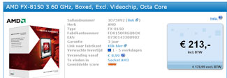
The new 8-core AMD FX-8150 Black Edition can already be spotted for a price as low as 213 EUR. Considering this product launched at 245 EUR 5 days ago, that's quiite a difference.


» Read full story

Intel Xeon E5 Sandy Bridge-E CPUs Launch Schedule

Processor 721 Published by Hilbert Hagedoorn 0

At this year's IDF conference, Intel made public the fact that it has delayed the arrival of its first Xeon E5 server processors, but nobody back then knew when these CPUs will arrive. A recent report however has managed to uncover the chip maker's plans regarding this new series of CPUs as SoftPedia reports today:

Previously, the Xeon E5 product families were scheduled for a Q4 2011 release, but CPU World has find out that Intel's current roadmaps place the launch of these chips in the second Q1 of 2012.

Just as their naming scheme implies, Xeon E5-1600 CPUs are to be installed in uni-processor machines while products in the Xeon E5-2600 range support dual-socket configurations.

Despite this difference, both of these Xeon CPU series will be compatible with Intel's socket R motherboards (LGA-2011).

Just like their desktop counterparts, the CPUs released in the Xeon 2600-series will feature HyperThreading, Turbo Boost technology, as well as the AVX and AES instructions, but they will also receive support for VT-x / VT-d / VT-c virtualization.

Next to the Xeon E5-2600 series, Intel also plans to release the Xeon E5-2400 processor family which also supports dual-socket systems and is compatible with LGA-1356 motherboards (socket B2).

As the E5-2400 processors will be based on the Sandy Bridge-EN architecture, they carry a tri-channel memory controller, compared to the quad-channel controller available in LGA-2011 chips.

Together with these three processor series, Intel will also introduce a quad-socket version of the Sandy Bridge-EP, dubbed the E5-4600, the launch of which has now been postponed for the second quarter of 2012.

All Xeon E5 processors will use the C600 chipset, code-name Patsburg, that we detailed in a previous report.

Sandy Bridge-EN and Sandy Bridge-EP CPUs feature as much as eight processing cores, pack up to 20MB of shared L3 cache, have a TDP rated between 80W and 150W, and support one or two Quick Path Interconnect links, depending on the model.


» Read full story

AMD FX watercooling kit gets pictured

Processor 721 Published by Hilbert Hagedoorn 0

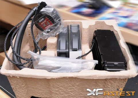
I just got an email from AMD yesterday evening that AMD is shipping out coolign kits to reviewers, this must be it. A watercooling bundle for AMD's 8-core FX "Bulldozer" chips. It's unknown which models will be available with this cooler, which looks rather similar to the Antec Kuhler H2O 920.

The Asian site XFastet has posted up four pictures of the new water cooler that AMD will be offering for improved cooling of the new 8-core processors.


» Read full story

Intel discontinues some LGA775 and LGA1156 chips

Processor 721 Published by Hilbert Hagedoorn 0

Intel has discontinued a couple more processors. It includes the Core i5-661 and Core i3-530 LGA1156 models, and the Pentium E5700, Celeron E3500 and E3400 (boxed only for the latter) LGA775 chips.

The Core i5-661 and Core i3-530 will be available for orders until April 27, 2012 and will continue shipping until October 5th, 2012, for the tray versions, and until supplies are depleted, for the boxed SKUs.

Orders for the Pentium E5700 and Celeron E3500 will be halted on December 30th, 2011, while shipments are slated to go on until June 8th, 2012 (tray) or while supplies last (boxed). As for the boxed Celeron E3400, it will also be up for order until December 30th (2011) and will ship until there are no more units in Intel's warehouses.


» Read full story

AMD Opteron 4200 series arrive

Processor 721 Published by Hilbert Hagedoorn 0

Check out the AMD Opteron 4200 series. It includes eight Valencia-based processors, four with six cores and another four with eight cores.

Like Opteron 4100 family, 4200 family is a mix of standard-, mid- and low-power microprocessors. The only known at this time low-power "Valencia" model is Opteron 4256 EE. This eight-core part runs at 2.5 GHz, and has 32 Watt Average CPU Power, which, we believe, corresponds to 35W TDP.

Two mid-power Opterons are six-core 4228 HE and eight-core 4274 HE. These processors come with 2.8 GHz and 2.5 GHz clock speeds, and they both boast 50W ACP (65W TDP).

All remaining models have 75 Watt ACP, or 95 Watt TDP. Opteron 4226, 4234 and 4238 have 6 CPU cores, and operate at 2.7 GHz, 3.1 GHz and 3.3 GHz. Opteron 4280 and 4284 have 8 cores, although their clock frequencies are lower, only 2.8 GHz and 3 GHz.

Model # Cores Frequency ACP
Opteron 4226 6 cores 2.7 GHz 75 Watt
Opteron 4228 HE 6 cores 2.8 GHz 50 Watt
Opteron 4234 6 cores 3.1 GHz 75 Watt
Opteron 4238 6 cores 3.3 GHz 75 Watt
Opteron 4256 EE 8 cores 2.5 GHz 32 Watt
Opteron 4274 HE 8 cores 2.5 GHz 50 Watt
Opteron 4280 8 cores 2.8 GHz 75 Watt
Opteron 4284 8 cores 3 GHz 75 Watt


» Read full story

Intel 32nm Atom chips get specifications

Processor 721 Published by Hilbert Hagedoorn 0

Here are the official specifications of Intel's new 32nm "Cedarview" Atom processors. Here's an overview, the CPU frequency range refers to Burst Mode, which is a Turbo-like feature.

  • D2500: 1.86 - 2.13GHz clockspeed, 400MHz GPU, 10W TDP
  • D2700: 2.13 - 2.4GHz clockspeed, 640MHz GPU, 10W TDP
  • N2600: 1.6 - 1.86GHz clockspeed, 400MHz GPU, 3.5W TDP
  • N2800: 1.86 - 2.13GHz clockspeed, 640MHz GPU, 6.5W TDP

» Read full story

AMD Bulldozer FX-Series Launch Date Confirmed

Processor 721 Published by Hilbert Hagedoorn 0

US-based computer retailer Micro Center has confirmed the launch date of AMD's next-generation FX-Series processors based on the high-performance Bulldozer architecture, which are expected to arrive on October 12.

"AMD is launching their new AM3+ FX series processors on 10/12/11. We currently have a number of AM3 + compatible motherboards in stock. These motherboards will support the new AM3 + FX processors as well as legacy AM3 processors."

The initial launch will include six FX-Series processors, four of them featuring eight processing cores while the two other include six and respectively four cores.

The fastest of these upcoming chips is called the FX-8150 and it sports a base frequency of 3.6GHz, a maximum Turbo frequency of 4.2GHz, 8MB of Level 2 cache memory, and has a TDP of 125W.

Right bellow this CPU stands the FX-8120 that also packs eight processing cores and other similar features, but comes clocked at 3.1GHz (4GHz in Turbo mode).

The FX-8120 will also be the only AMD FX-Series processor to be available in two different SKUs, one featuring a 125W TDP while the other is a 95W part.

The three remaining processors are the FX-8100, which has a base frequency of 2.8GHz and a maximum Turbo frequency of 3.7GHz, the six-core FX-6100 with a 3.3GHz base speed, 3.8GHz Turbo and 6MB of Level 2 cache memory and the quad-core FX-4100, which is clocked at 3.6GHz and can reach 3.8GHz when Turbo Core is active.


» Read full story

Intel Sandy Bridge-E to get C2 stepping after launch

Processor 721 Published by Hilbert Hagedoorn 0

Intel's Sandy Bridge-E will get a C2 stepping likely sometime near the very end of the year. This new stepping will fix issues with VT-d, vr-zone:

We knew that Intel's Sandy Bridge-E chips were big and complicated to make, but what we didn't expect was that Intel was going to continuously keep running into problems. The current C1 stepping is apparently having problems with VT-d, not a major issue for most consumers' maybe, but it's a huge problem when it comes to Xeon chips and as such Intel is working on the C2 stepping to fix this "errata".

The only good news here for Intel, if you look at that way, is that its current Extreme Edition CPU's don't support VT-d, neither does the Sandy Bridge K-SKU CPU's, so as far as the consumer platform is concerned it looks like there won't be any further delays, but the initial batch should be C1 stepping rather than C2. The C1 stepping should be in production by now, or by the latest by next week, although we don't know when Intel will kick off production of the C2 stepping, but it's very possible it won't be until next year as qualification samples of the C2 stepping isn't expected until the very end of the year


» Read full story

AMD Piledriver 10 percent faster than Bulldozer?

Processor 721 Published by Hilbert Hagedoorn 0

A leaked slide claimed to originate from AMD claims Bulldozer will be succeeded by Piledriver. Dubbed FX Next, this next-gen chip is claimed to offer a 10 percent increase in x86 performance compared to Bulldozer.

What's new in Piledriver? According to the slide, a 10% increase in x86 performance. Version 3.0 of Turbo Core is also on the menu, as are a couple of new instructions. FX Next will reportedly use the same AM3+ socket as the first wave of Bulldozer CPUs, so you should be able to pop it into existing motherboards.

The AMD slide suggests that FX Next will use the same 9-series chipsets that have been around since May. Those chipsets are actually just rebranded versions of AMD's old 8-series gear, which has been gracing motherboards for a year and a half now. That means no native USB 3.0 support and a slower 6Gbps SATA controller than competing Intel platforms. The 990FX does offer gobs of PCI Express 2.0 connectivity, but that's gonna look dated if PCIe 3.0 hardware starts popping up next year.


» Read full story

Designer Behind the World's First Microprocessor

Processor 721 Published by Hilbert Hagedoorn 0

Federico Faggin visited Intel headquarters in late summer of 2011 to share memories from 40 years ago, when teamed up with Ted Hoff and Stan Mazur to create Intel's 4004 chip, which became the world's first single chip microprocessor.

Faggin talks about the day in January 1971, when he first tested the chip and it worked flawlessly. That was the day the microprocessor was born, he says, and today it is at the heart of the Internet revolution. He says the microprocessor has become the tiny speck of intelligence that converges communication, computing and control capabilities, connecting all of our devices from computers to small smartphones.

He has his eye on quantum computing as the next frontier of computing because of potential is beyond what capable with today's mechanical microprocessors. Yet he believes computing will never rival the complexity and capabilities on human intelligence.


» Read full story

AMD is suffering from poor Llano yields

Processor 721 Published by Hilbert Hagedoorn 0

Guru3D.com ImageAMD send out a profit warning to investors, stating it won't be able to achieve the previously forecasted 8-12 percent rise in quarterly revenue due to Llano manufacturing issues at GlobalFoundries. Third quarter revenue is anticipated to increase four to six percent compared to the second quarter, and the company also reveals that its Interlagos server processor shipped later than originally anticipated.

AMD (NYSE: AMD) today announced that revenue for the third quarter ending Oct. 1, 2011 is expected to increase four to six percent as compared to the second quarter of 2011. The company previously forecasted third quarter 2011 revenue to increase 10 percent, plus or minus two percent, from the second quarter of 2011.

In addition, AMD expects third quarter gross margin to be approximately 44 to 45 percent. The company previously forecasted third quarter 2011 gross margin to be approximately 47 percent.

The less-than-forecasted preliminary third quarter 2011 revenue results are primarily due to 32 nanometer (nm) yield, ramp and manufacturing issues at GLOBALFOUNDRIES in its Dresden, Germany factory that limited supply of "Llano". Additionally, 45nm supply was less than expected due to complexities related to the use of common tools across both technology nodes. AMD continues to work closely with its key partner GLOBALFOUNDRIES to improve 32nm yield performance in order to satisfy strong demand for AMD products.

The less-than-forecasted preliminary third quarter 2011 gross margin results are primarily due to less-than-expected supply of "Llano" and associated products with higher average selling price (ASP). Additionally, shipments of AMD's next-generation server processor, codenamed "Interlagos", occurred later in the third quarter than originally anticipated.

AMD will report third quarter 2011 results after market close on Thursday, Oct. 27, 2011. AMD will hold a conference call for the financial community at 2:00 p.m. PT (5:00 p.m. ET) that day to discuss third quarter financial results and to provide information regarding expected fourth quarter results. AMD will provide a real-time audio broadcast of the teleconference on the Investor Relations page at http://www.amd.com. The webcast will be available for 10 days after the conference call.


» Read full story

AMD 2012 and 2013 Fusion roadmap leak

Processor 721 Published by Hilbert Hagedoorn 0

New details have been leaked about AMD's 2012 and 2013 Fusion roadmap. It shows that AMD likely has already shipped engineering samples of its Llano refresh "Trinity". Trinity prospect launch date is January 2012. Its chips will be branded E2s, A4s, A6s, or A8s. It will come with a graphics refresh ("London"/Northern Islands) and will swap the "Husky" cores for "Piledriver" cores -- "enhanced" versions of AMD's new 32 nm Bulldozer architecture.

Confusingly, Trinity's platform has yet two more code-name -- "Comal" for laptops and "Virgo" for desktops -- and the slides point to it being sold alongside Llano for Q1 2012, with Llano being phased out by Q2 2012. This may create some market confusion as both the new and the old chips will share the same A-Series branding.

Click on the thumbnail.


» Read full story